

Organic light emitting display device
a display device and light-emitting technology, applied in semiconductor devices, instruments, computing, etc., can solve the problems of difficult attachment of touch panel drive ic to flexible printed circuit boards, compatibility issues between products, etc., and achieve the effect of increasing the thickness of the display devi
- Summary
- Abstract
- Description
- Claims
- Application Information
AI Technical Summary
Benefits of technology
Problems solved by technology
Method used
Image

Examples
first embodiment
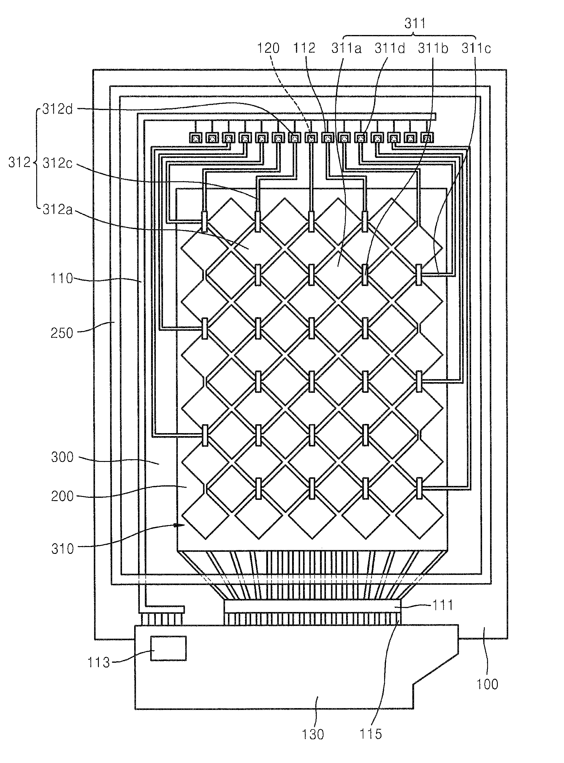
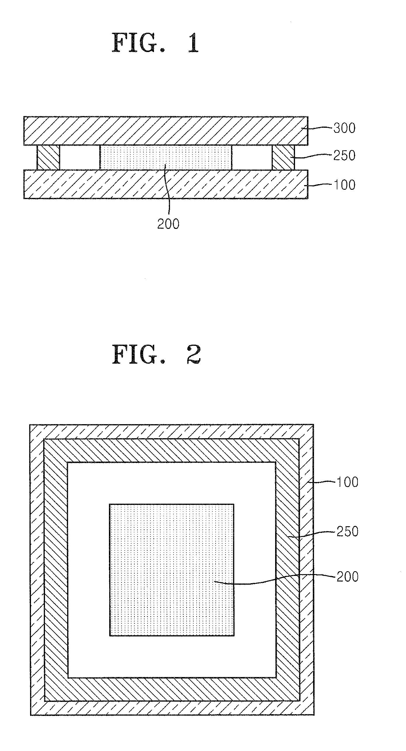
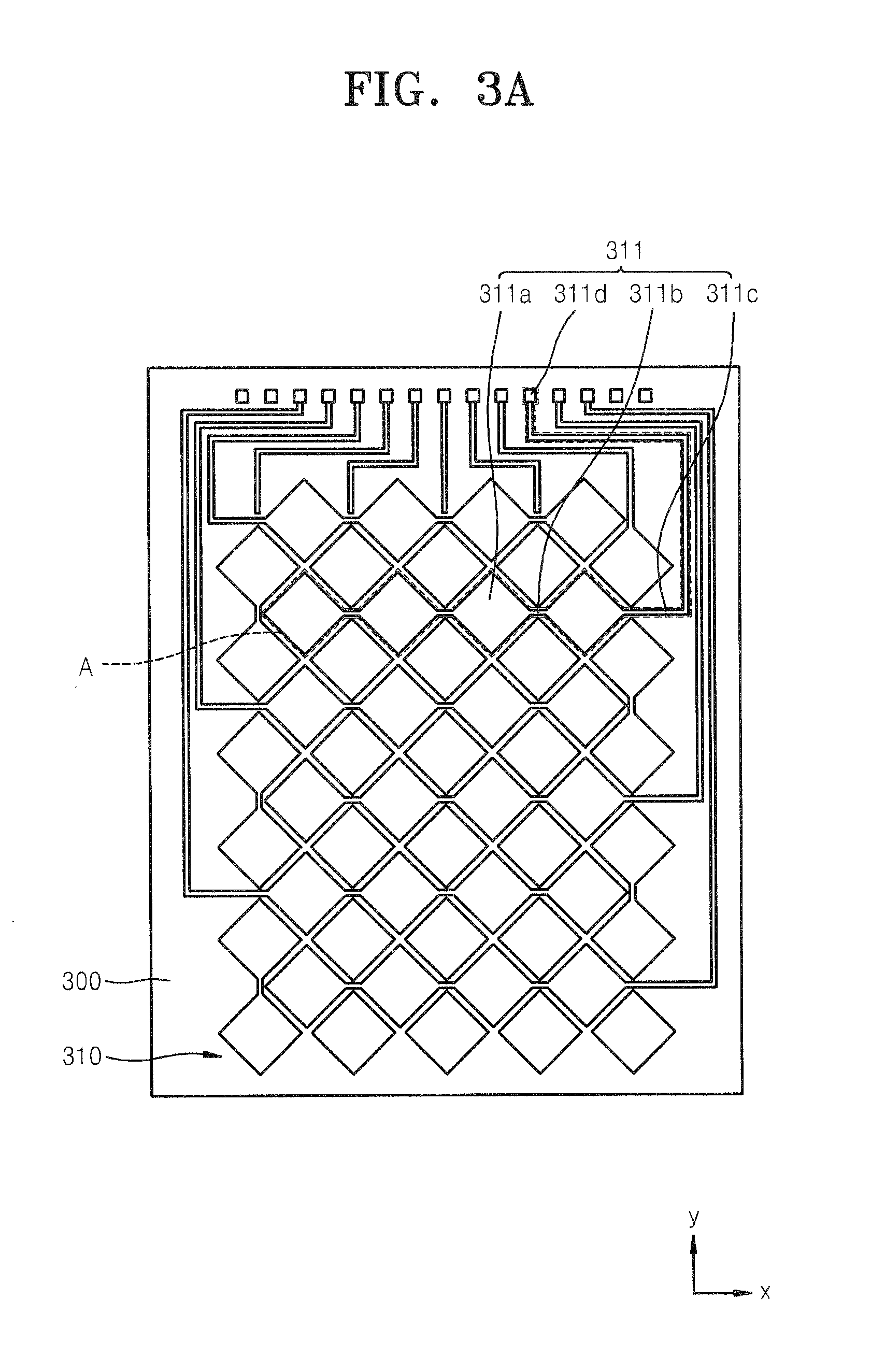
[0046]FIG. 1 is a cross-sectional schematic view of a portion of an organic light emitting display device according to a first embodiment of the present invention, and FIG. 2 is a plan schematic view of the organic light emitting display device of FIG. 1. In FIG. 2, an encapsulation substrate 300 illustrated in FIG. 1 is not shown.
[0047]Referring to FIGS. 1 and 2, a display unit 200 including a plurality of organic light emitting diodes (OLEDs) is formed on a substrate 100.
[0048]The substrate 100 may be formed of transparent glass containing SiO2 as a main component, but is not limited thereto, and thus may also be formed of a transparent plastic material that may be an insulating organic material selected from the group consisting of polyethersulphone (PES), polyacrylate (PAR), polyetherimide (PEI), polyethyelene napthalate (PEN), polyethyelene terephthalate (PET), polyphenylene sulfide (PPS), polyallylate, polyimide, polycarbonate (PC), triacetate cellulose (TAC), cellulose acetat...
second embodiment
[0092]FIG. 7A is a bottom schematic view of an encapsulation substrate and a first pattern layer formed on a surface of the encapsulation substrate in an organic light emitting display device according to a second embodiment of the present invention.
[0093]FIG. 7B is a bottom view of the first pattern layer of FIG. 7A, and a second pattern layer on the first pattern layer. FIG. 7C is a cross-sectional schematic view taken along line VII-VII in FIG. 7B. FIG. 7D is a bottom perspective schematic view of the first pattern layer and the second pattern layer of FIG. 7B.
[0094]Referring to FIGS. 7A through 7D, a first pattern layer 410, a first insulating layer 430, a second pattern layer 420, and a second insulating layer 440 are sequentially formed on a surface of an encapsulation substrate 400, respectively, to face a substrate.
[0095]In the embodiment illustrated in FIGS. 7A through 7D, the first and second direction pattern units are not formed using a single pattern layer. Instead, the...
third embodiment
[0105]FIGS. 8A and 8B are plan (or top) schematic views of an encapsulation substrate 500 and a first pattern layer formed on a surface of the encapsulation substrate 500 in an organic light emitting display device according to a third embodiment of the present invention. FIG. 8C is a plan (or top) schematic view of the first pattern layer of FIGS. 8A and 8B, and a second pattern layer on the first pattern layer. FIG. 8D is a cross-sectional schematic view taken along line VIII-VIII in FIG. 8C. FIG. 8E is a plan (or top) perspective schematic view of the first pattern layer and the second pattern layer of FIG. 8C.
[0106]Referring to FIGS. 8A through 8E, a first pattern layer 510, a first insulating layer 530, a second pattern layer 520, and a second insulating layer 540 are sequentially formed on a first side or surface (i.e., a top surface) of the encapsulation substrate 500, respective, to face away from a display unit 200 (see FIG. 10). Here, the encapsulating substrate 500 also h...
PUM
 Abstract
Description
Claims
Application Information