Phase change memory program method without over-reset

a program method and memory technology, applied in the field of memory devices, can solve problems such as insufficient resistance state change, and achieve the effect of avoiding unnecessarily high reset currents and avoiding over-res

Active Publication Date: 2010-05-06
MACRONIX INT CO LTD +1
View PDF100 Cites 14 Cited by
  • Summary
  • Abstract
  • Description
  • Claims
  • Application Information

AI Technical Summary

Benefits of technology

[0016]Reset operations described herein provide the current needed to induce a phase change to the higher resistance state for the memory cells of the array while also avoiding the use of unnecessarily high reset currents. Successive voltage pulses in the fixed sequence provide increasing current through the memory element of the memory cell until change to the higher resistance state occurs. Once the memory element is reset to the higher resistance state by a particular voltage pulse in the fixed sequence, the remaining voltage pulses in the fixed sequence are below the threshold voltage and thus insufficient to change the resistance state back from the higher resistance state to the lower resistance state. As a result, the memory cells of an array can be reset with a current near the necessary reset current and avoid over-reset.

Problems solved by technology

Once the memory element is reset to the higher resistance state by a particular voltage pulse in the fixed sequence, the remaining voltage pulses in the fixed sequence are below the threshold voltage and thus insufficient to change the resistance state back from the higher resistance state to the lower resistance state.

Method used


Image

  • Phase change memory program method without over-reset
  • Phase change memory program method without over-reset
  • Phase change memory program method without over-reset

Examples


first embodiment

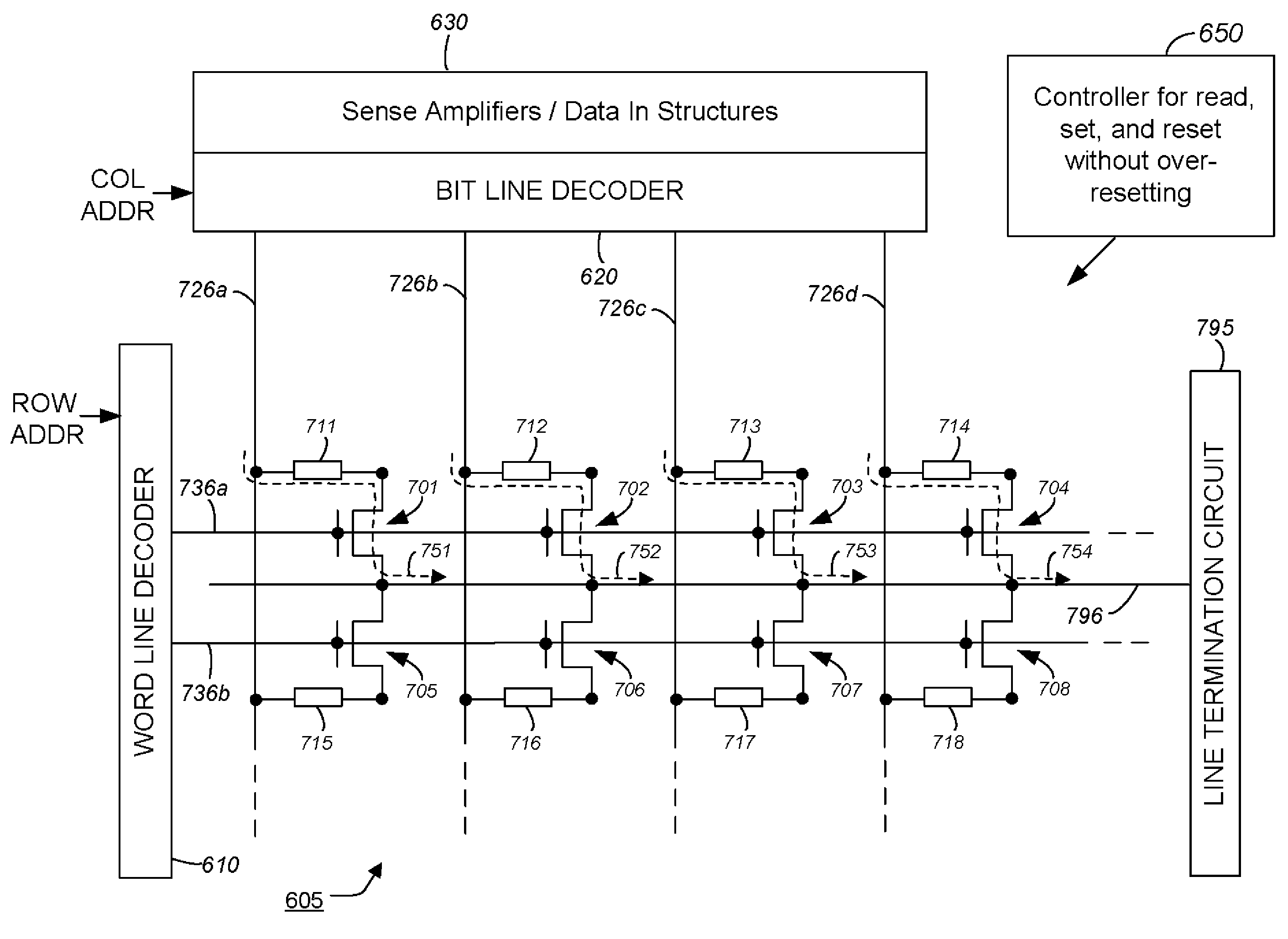
[0053]FIG. 7 illustrates a first embodiment for array 605 of the integrated circuit 600. As shown in the embodiment of FIG. 7, each of the memory cells of array 605 includes an field effect transistor access device, eight of which are shown as memory cells 701-708 having respective phase change memory elements 711-718 are illustrated in FIG. 7, representing a small section of an array that can include millions of memory cells. The memory elements are programmable to a plurality of resistance states including a high resistance state and at least one lower resistance state.

[0054]Sources of each of the access transistors of memory cells 711-718 are connected to common line 796 that terminates in a line termination circuit 795, such as a ground terminal. In another embodiment the sources of the access devices are not electrically connected, but independently controllable. The line termination circuit 795 may include bias circuits such as voltage sources and current sources, and decoding...

second embodiment

[0084]In the timing diagram of FIG. 10 the voltage pulses of increasing pulse height were applied between the word line 736a and the common line 796. FIG. 12 illustrates a timing diagram of the reset operation 900 of FIG. 9 in which the voltage pulses of increasing pulse height are applied between the bit line 726a and the common line 796.

[0085]In FIG. 12, a series of four control voltage pulses having substantially the same pulse height VWL sufficient to turn on the access transistor are applied to the word line 736a, and the common line 796 coupled to the source terminal is supplied a ground potential.

[0086]As can be seen in FIG. 12, the voltage on the bit line 726a increases in a stepped fashion between each of the control pulses applied to the word line 736a. Although the voltage on the bit line increases in a stepped fashion, as used herein the voltage on the bit line is considered to be a pulse when the control voltage pulse is sufficient turn on the access transistor and caus...

third embodiment

[0090]FIG. 14 illustrates the array in which the memory cells are implemented using diode access devices, and FIG. 15 illustrates a simplified timing diagram of the reset operation 900 of FIG. 9 for the memory cells of FIG. 14.

[0091]In the timing diagram of FIG. 15 the fixed sequence of voltage pulses of increasing pulse height are applied to the bit line 726a and the word line 736a is supplied a constant voltage (ground in this example). Thus, the voltage pulses of increasing pulse height are applied across the series arrangement of the diode and the memory element 711 for the memory cell 701 to cause increasing current in path 751 and through the memory element 711 until change to the higher resistance state occurs. Additionally, the voltage pulses in the fixed sequence are adapted to cause a voltage across the memory element 711 after the memory element 711 is in the higher resistance state that is less than the threshold voltage VTH. Thus, once the memory element 711 is in the h...


PUM


Abstract

Memory devices and methods for operating such devices are described herein. A method as described herein includes applying a fixed sequence of voltage pulses across the memory cell of increasing pulse height to change the resistance state from the lower resistance state to the higher resistance state. The fixed sequence of voltage pulses cause increasing current through the phase change memory element until change to the higher resistance state occurs, and after the change the voltage pulses in the fixed sequence causing a voltage across the phase change memory element less than the threshold voltage.

Description

PARTIES TO A JOINT RESEARCH AGREEMENT[0001]International Business Machines Corporation, a New York corporation, and Macronix International Corporation, Ltd., a Taiwan corporation, are parties to a Joint Research Agreement.BACKGROUND OF THE INVENTION[0002]1. Field of the Invention[0003]The present invention relates to memory devices based on phase change based memory materials, and to methods for operating such devices.[0004]2. Description of Related Art[0005]Phase change based memory materials, like chalcogenide based materials and similar materials, can be caused to change phase between an amorphous state and a crystalline state by application of electrical current at levels suitable for implementation in integrated circuits. The generally amorphous state is characterized by higher electrical resistivity than the generally crystalline state, which can be readily sensed to indicate data. These properties have generated interest in using programmable resistive material to form nonvol...

Claims


Application Information

Patent Timeline
Patent Type & Authority Applications(United States)
IPC IPC(8): G11C11/00
CPCG11C13/0004G11C13/0069G11C2013/0071G11C2013/009
Inventor LEE, MING-HSIUBREITWISCH, MATTHEW J.LAM, CHUNG HON
Owner MACRONIX INT CO LTD
Why Eureka
Try Eureka