Layout verification apparatus, layout apparatus, layout verification method, layout verification program, and wiring forming method

a layout verification and layout technology, applied in the field of layout verification apparatus layout verification program, layout verification method, etc., can solve the problems of difficult to correct the layout and wiring data without changing, difficult to cover completely, and difficult to perform accurate verification

Inactive Publication Date: 2010-05-13
RENESAS ELECTRONICS CORP
View PDF1 Cites 9 Cited by
  • Summary
  • Abstract
  • Description
  • Claims
  • Application Information

AI Technical Summary

Benefits of technology

[0020]According to the present invention, it is possible to provide a layout verification apparatus, a layout apparatus, a layout verification program, and a wiring forming method, each of which enables correction of the layout and wiring data without changing the position of the terminal even if the method of detecting the defect part based on a result of the simulation is used.

Problems solved by technology

However, it is difficult to cover completely the layout results to be the defect patterns.
In other words, it is difficult to perform accurate verification by the technology of Patent Document 1.
In other words, there is a problem that if the method of detecting the defect part based on the mask data is used, it becomes difficult to correct the layout and wiring data without changing the position of the terminal included in the primitive cell.

Method used


Image

  • Layout verification apparatus, layout apparatus, layout verification method, layout verification program, and wiring forming method
  • Layout verification apparatus, layout apparatus, layout verification method, layout verification program, and wiring forming method
  • Layout verification apparatus, layout apparatus, layout verification method, layout verification program, and wiring forming method

Examples


Embodiment Construction

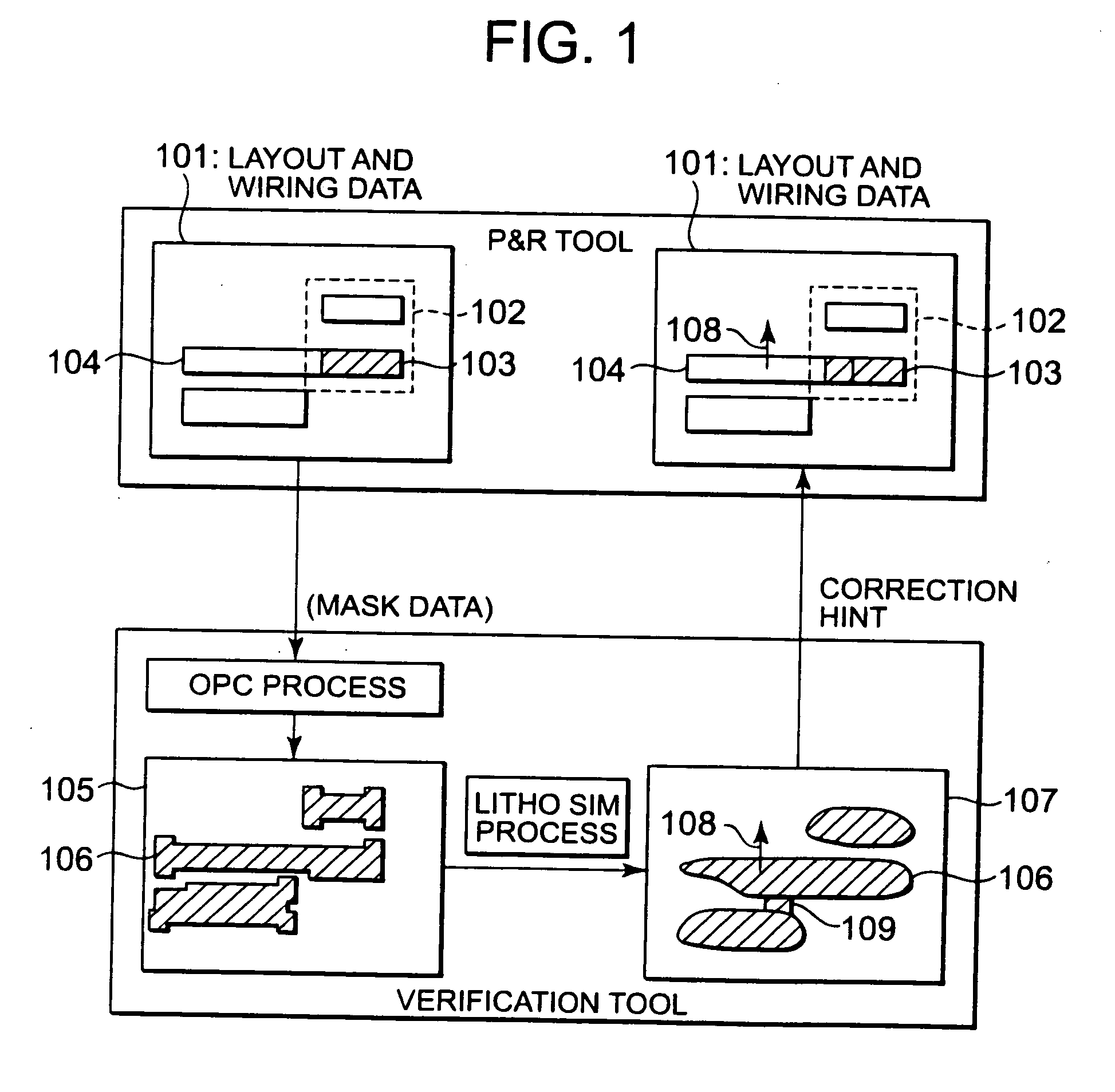
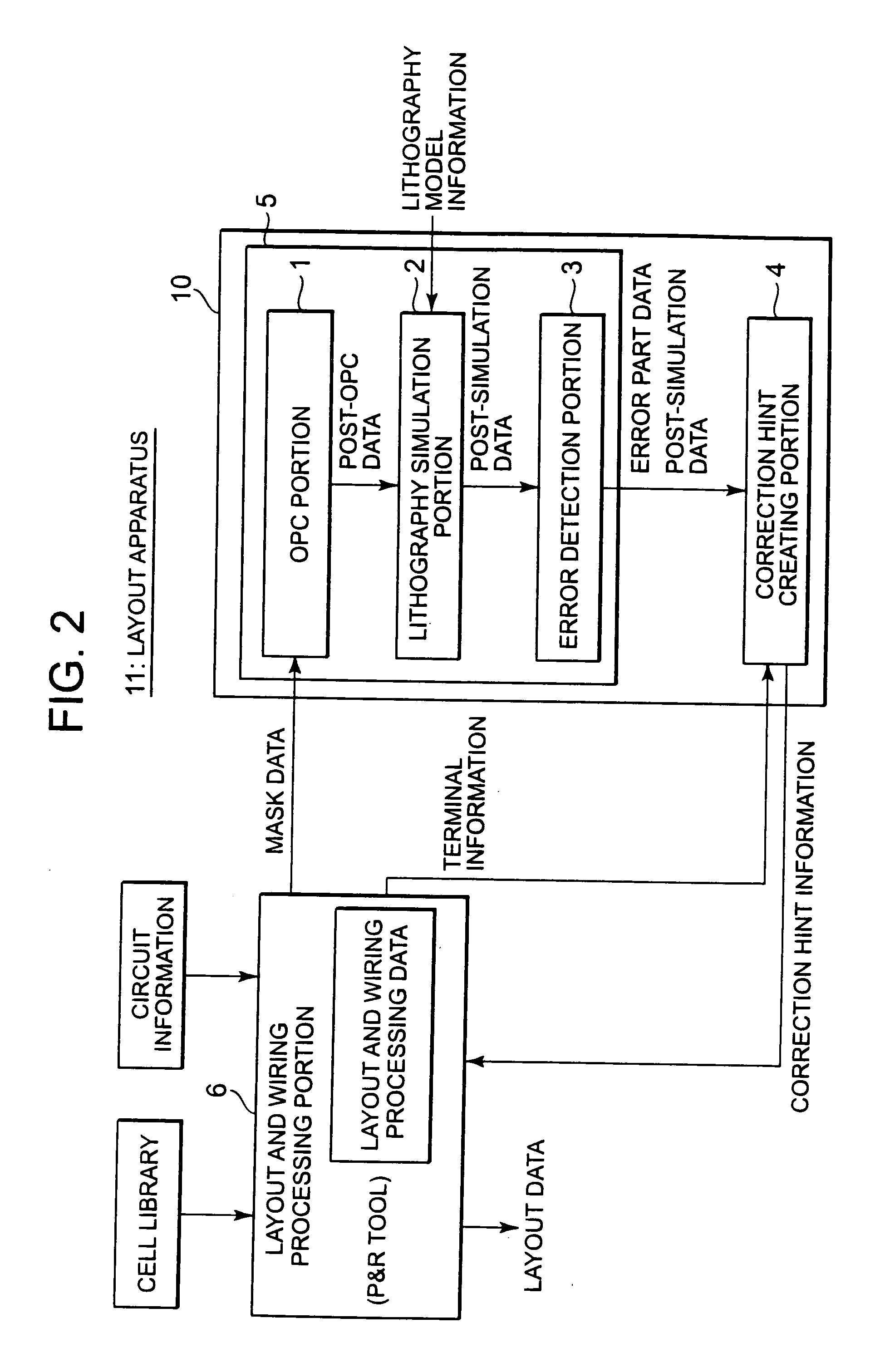
[0034]Now, an embodiment of the present invention is described with reference to the attached drawings. FIG. 2 is a schematic block diagram illustrating a layout apparatus 11 according to this embodiment.

[0035]As illustrated in FIG. 2, the layout apparatus 11 includes a layout and wiring processing portion 6 for performing a layout and wiring process, and a layout verification apparatus 10 for performing verification of the layout. The layout verification apparatus 10 includes a verification portion 5 and a correction hint creating portion 4. The verification portion 5 includes an optical proximity correction (OPC) portion 1, a lithography simulation portion 2, and an error detection portion 3.

[0036]The layout and wiring processing portion 6 and the layout verification apparatus 10 are realized by central processing means (CPU) executing a layout program installed in a computer. In particular, the layout verification apparatus 10 is realized by a layout verification program containe...


PUM

PropertyMeasurementUnit
optical proximity correctionaaaaaaaaaa
widthaaaaaaaaaa
optical proximityaaaaaaaaaa

Abstract

The layout verification apparatus includes: a verification unit for obtaining mask data indicating a mask pattern to be drawn on a mask based on layout and wiring data indicating positions of a group of primitive cells and positions of connection wires connected to the group of primitive cells, and for verifying a position of the mask pattern based on the mask data, so as to detect an error part; and a correction hint creating unit for creating correction hint information based on the error part, and for sending the correction hint information to a layout and wiring unit for correcting the layout and wiring data. The correction hint creating unit obtains terminal information indicating positions of a group of terminals included in the group of primitive cells and creates the correction hint information based on the terminal information so that the positions of the group of terminals are not changed by the layout and wiring unit.

Description

BACKGROUND OF THE INVENTION[0001]1. Field of the Invention[0002]The present invention relates to a layout verification apparatus, a layout apparatus, a layout verification method, a layout verification program, and a wiring forming method.[0003]2. Description of the Related Art[0004]When a circuit such as a semiconductor integrated circuit is manufactured, a layout pattern thereof is designed first. After that, a photomask (hereinafter, referred simply to as a mask) is created based on the layout pattern. A pattern drawn on the mask is transferred onto a substrate, and thus an actual circuit is obtained.[0005]When the layout pattern is designed, in the first place, positions of a group of primitive cells are determined, and positions of a group of wirings connecting the primitive cells are determined so that a desired circuit operation may be obtained. Thus, layout and wiring data is obtained. A pattern drawn on the mask is not always identical to a pattern formed actually on the su...

Claims


Application Information

Patent Timeline
Patent Type & Authority Applications(United States)
IPC IPC(8): H01R43/00G06F17/50
CPCY10T29/49117G06F17/5081G06F30/398
Inventor HAMAMOTO, TAKESHI
Owner RENESAS ELECTRONICS CORP
Why Eureka
Try Eureka