
Extremely stretchable electronics

a technology of integrated circuits and electronics, applied in the direction of contact member manufacturing, semiconductor/solid-state device details, conductors, etc., can solve the problems of brittle single-crystalline semiconductor materials and inability to withstand strains of more than about +/2%

Active Publication Date: 2010-05-13
MEDIDATA SOLUTIONS
View PDF63 Cites 140 Cited by
  • Summary
  • Abstract
  • Description
  • Claims
  • Application Information

AI Technical Summary

Benefits of technology

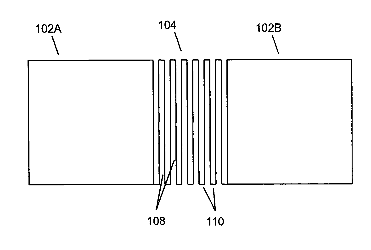
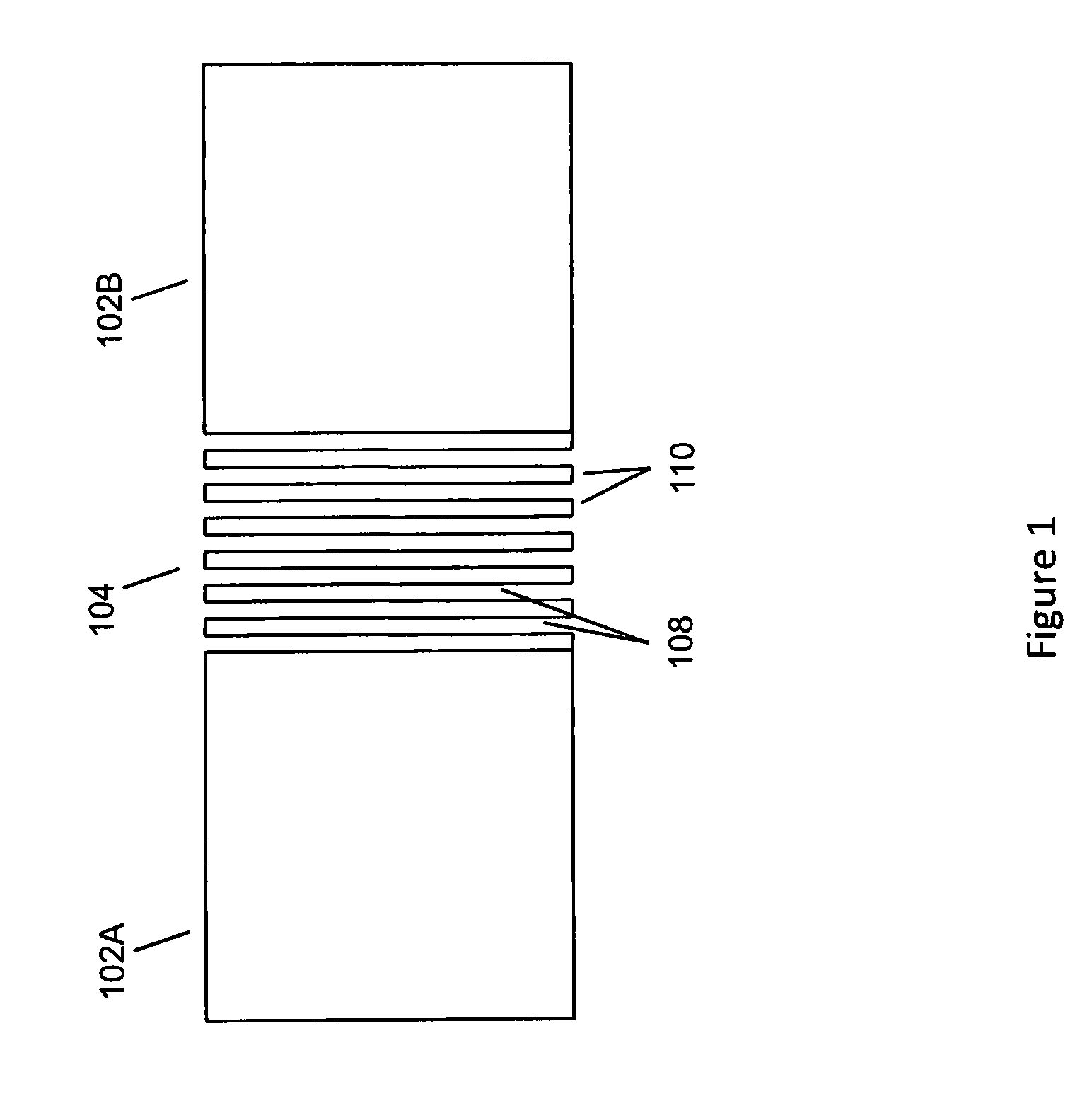
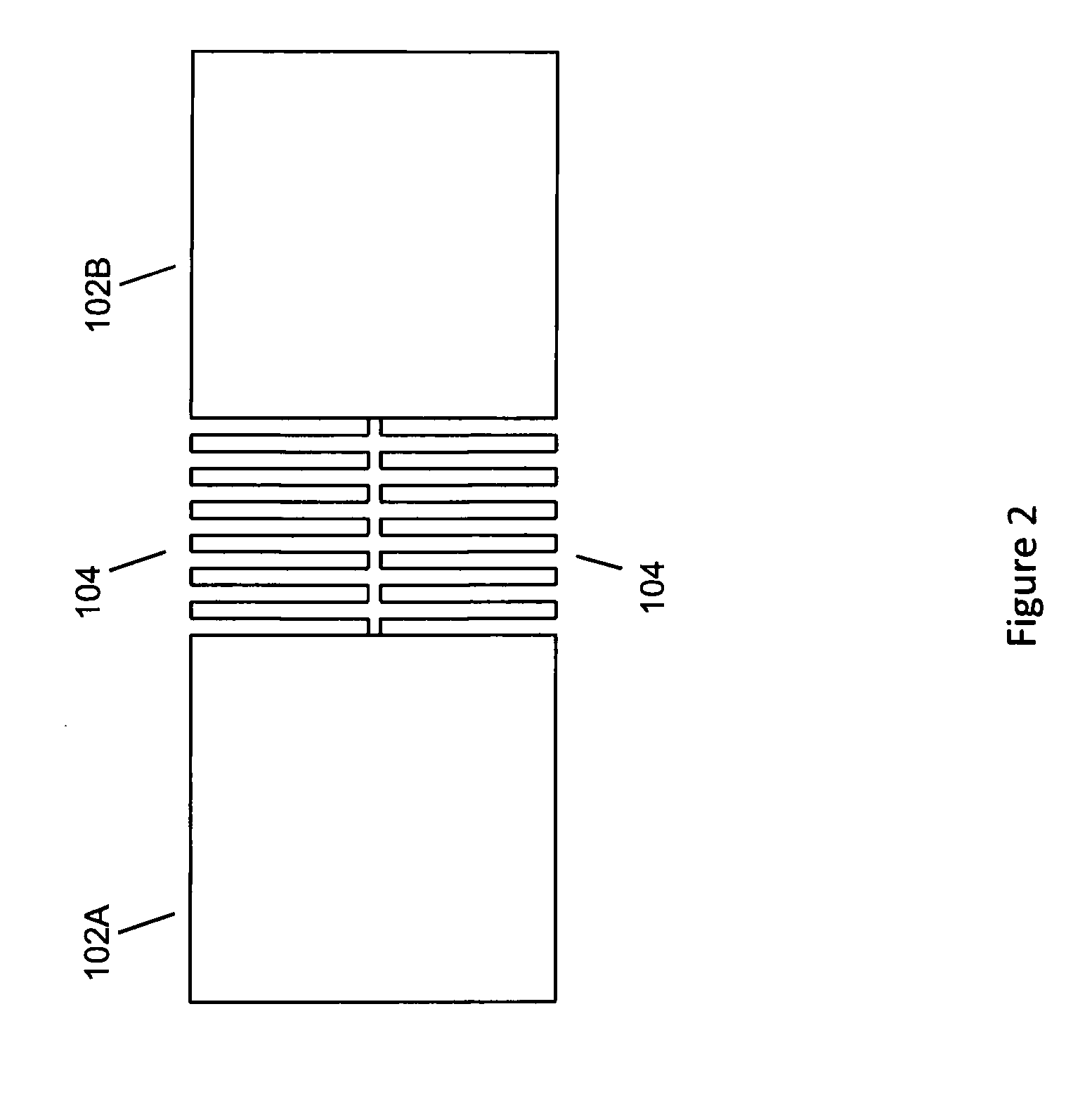
[0005]In embodiments, the stretching and compressing may be accomplished by fabricating integrated circuits (ICs) out of thin membrane single crystal semiconductors, which are formed into “islands” that are mechanically and electrically connected by “interconnects,” and transferring said ICs onto an elastomeric substrate capable of stretching and compressing. The islands are regions of non-stretchable / compressible ICs, while the interconnects are regions of material formed in a way to be highly stretchable / compressible. The underlying elastomeric substrate is much more compliant than the islands, so that minimal strain is transferred into the islands while the majority of the strain is transferred to the interconnects, which only contain electrical connections and not ICs. Each interconnect attaches one island to another island, and is capable of accommodating strain between the two aforementioned islands, including translation, rotation, or a combination of translation with rotation of one island relative to another. Even though the interconnects may be made of a rigid material, they act like weak springs rather than rigid plates or beams. This configuration thereby allows for the making of extremely stretchable electronics.

Problems solved by technology

For example, single crystal semiconductor materials are brittle and cannot typically withstand strains of greater than about + / −2%.

Method used


Image

  • Extremely stretchable electronics
  • Extremely stretchable electronics
  • Extremely stretchable electronics

Examples


Embodiment Construction

[0019]The present invention accomplishes extremely stretchable electronics by forming the electronics on discrete islands 102 of silicon.

[0020]With reference to the present invention, the term “stretchable”, and roots and derivations thereof, when used to modify circuitry or components thereof is meant to encompass circuitry that comprises components having soft or elastic properties capable of being made longer or wider without tearing or breaking, and it is also meant to encompass circuitry having components (whether or not the components themselves are individually stretchable as stated above) that are configured in such a way so as to accommodate and remain functional when applied to a stretchable, inflatable, or otherwise expandable surface. The term “expandable”, and roots and derivations thereof, when used to modify circuitry or components thereof is also meant to have the meaning ascribed above. Thus, “stretch” and “expand”, and all derivations thereof, may be used interchan...


PUM

PropertyMeasurementUnit
Fractionaaaaaaaaaa
Fractionaaaaaaaaaa
Fractionaaaaaaaaaa

Abstract

In embodiments, the present invention may attach at least two isolated electronic components to an elastomeric substrate, and arrange an electrical interconnection between the components in a boustrophedonic pattern interconnecting the two isolated electronic components with the electrical interconnection. The elastomeric substrate may then be stretched such that the components separate relative to one another, where the electrical interconnection maintains substantially identical electrical performance characteristics during stretching, and where the stretching may extend the separation distance between the electrical components to many times that of the unstretched distance.

Description

CROSS-REFERENCE TO RELATED APPLICATIONS[0001]This application claims the benefit of U.S. Provisional Application No. 61 / 113,622 entitled “Extremely Stretchable Interconnects” filed on Nov. 12, 2008, the entirety of which is incorporated herein by reference. Also, this application is a continuation-in-part of, and claims the benefit of United States Non-Provisional application Ser. No. 12 / 575,008, entitled “Catheter Balloon Having Stretchable Integrated Circuitry and Sensor Array” filed on Oct. 7, 2009, the entirety of which is incorporated herein by reference. application Ser. No. 12 / 575,008 claimed the priority of U.S. Provisional Application Nos. 61 / 103,361, filed Oct. 7, 2008 and 61 / 113,007, filed Nov. 10, 2008 the entirety of each of which is incorporated herein by reference.FIELD OF THE INVENTION[0002]The present invention relates to systems, apparatuses, and methods utilizing expandable or stretchable integrated circuitry, and more particularly to extremely stretchable integra...

Claims


Application Information

Patent Timeline
IPC IPC(8): H01B5/00H01L21/768H05K3/00H05K3/30H05K13/00
CPCY10T29/4913H05K2201/10106Y10T29/49204A61F2/958H01L23/4985H01L23/52Y10T29/49155H05K2201/09263H01L23/564H01L2924/0002H05K1/0283H05K1/189H05K3/326H01L23/528H05K1/00H01L23/3121H01L25/16H01L2924/00
Inventor ARORA, WILLIAM J.GHAFFARI, ROOZBEH
Owner MEDIDATA SOLUTIONS
Learn More