Current-driven display device

a display device and current-driven technology, applied in the field of display devices, can solve the problems of difficult design of pixel circuits and drive circuits, difficulty in making current flow through tfts, and problems in current program schemes, so as to achieve stable the effect of simplifying the circuit and ensuring the stability of the potential of the third power supply wiring lin

Active Publication Date: 2010-05-13
SHARP KK
View PDF12 Cites 10 Cited by
  • Summary
  • Abstract
  • Description
  • Claims
  • Application Information

AI Technical Summary

Benefits of technology

[0030]According to the first aspect of the present invention, by applying a potential that places the drive element in a conducting state to the data line and controlling the first and fourth switching elements to a conducting state, a data potential is provided to the control terminal of the drive element and thus the drive element can always be set to a conducting state, regardless of a previous state of the pixel circuit. Hence, at the point in time when the third switching element is controlled to a conducting state, the drive element can be reliably set to a conducting state. Thus, when variations in the threshold voltage of the drive element are compensated for, the circuit can operate properly.
[0031]In addition, since the drive element can be initialized with any one of the third and fourth switching elements being maintained in a non-conducting state, the drive element can be initialized without connecting the first and second power supply wiring lines to the third power supply wiring line and thus the potential of the third power supply wiring line can always be stabilized. Furthermore, since initialization of the drive element is performed using the potential of the data line, a power supply wiring line for initialization does not need to be additionally provided and thus the circuit can be simplified.
[0032]According to the second aspect of the present invention, by applying a potential that places the drive element in a conducting state to the data line and controlling the fourth switching element to a conducting state, a data potential is provided to the control terminal of the drive element and thus the drive element can always be set to a conducting state, regardless of a previous state of the pixel circuit. Hence, at the point in time when the third switching element is controlled to a conducting state, the drive element can be reliably set to a conducting state. Thus, when variations in the threshold voltage of the drive element are compensated for, the circuit can operate properly.
[0033]In addition, since the drive element can be initialized with any one of the third and fourth switching elements being maintained in a non-conducting state, the drive elemen...

Problems solved by technology

Hence, it is difficult to make currents flowing through TFTs and an organic EL element match each other between a large number of pixel circuits included in a display.
However, the current program scheme has problems.
Firstly, since a very small amount of current is handled, it is difficult to design a pixel circuit and...

Method used


Image

  • Current-driven display device
  • Current-driven display device
  • Current-driven display device

Examples


first embodiment

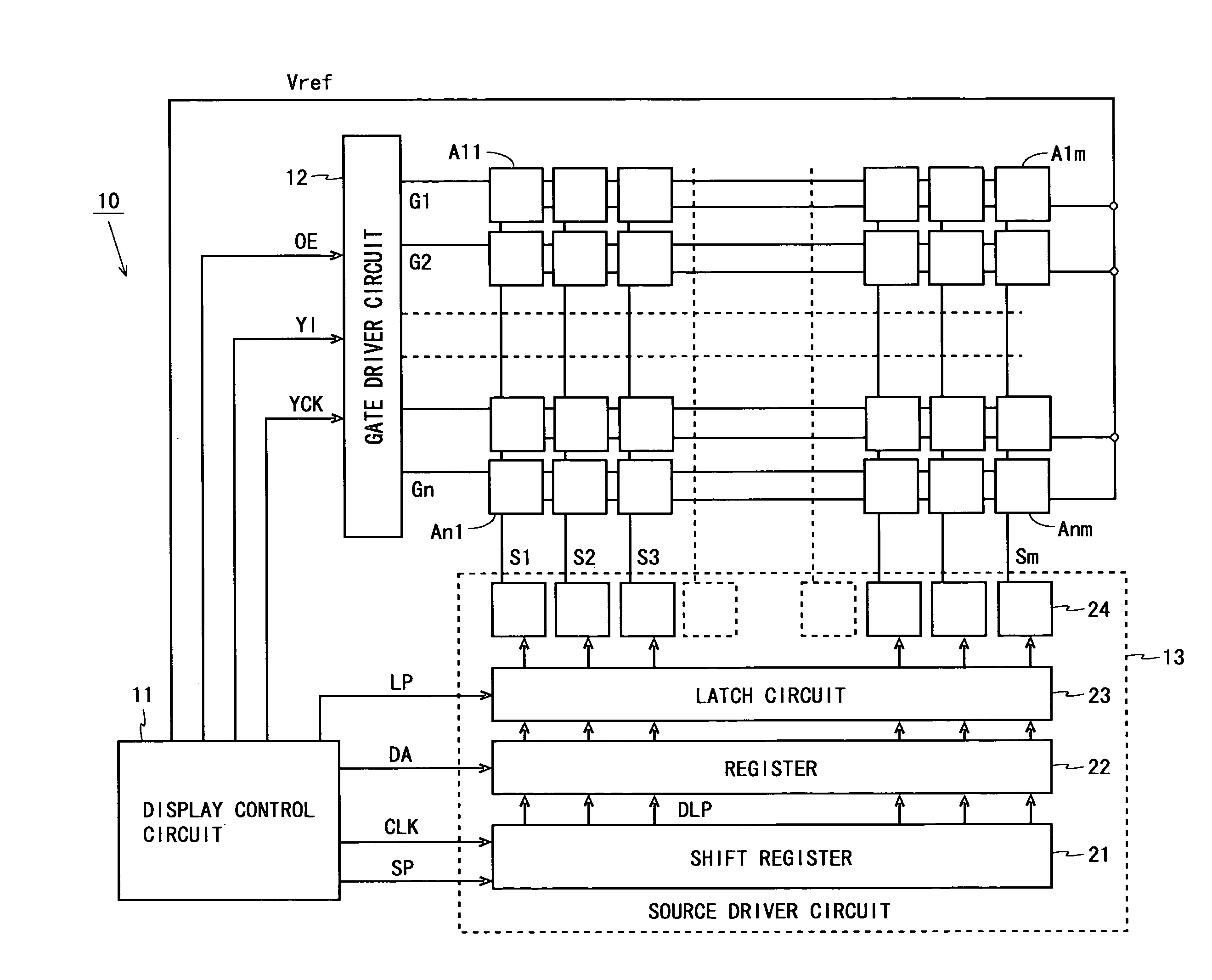
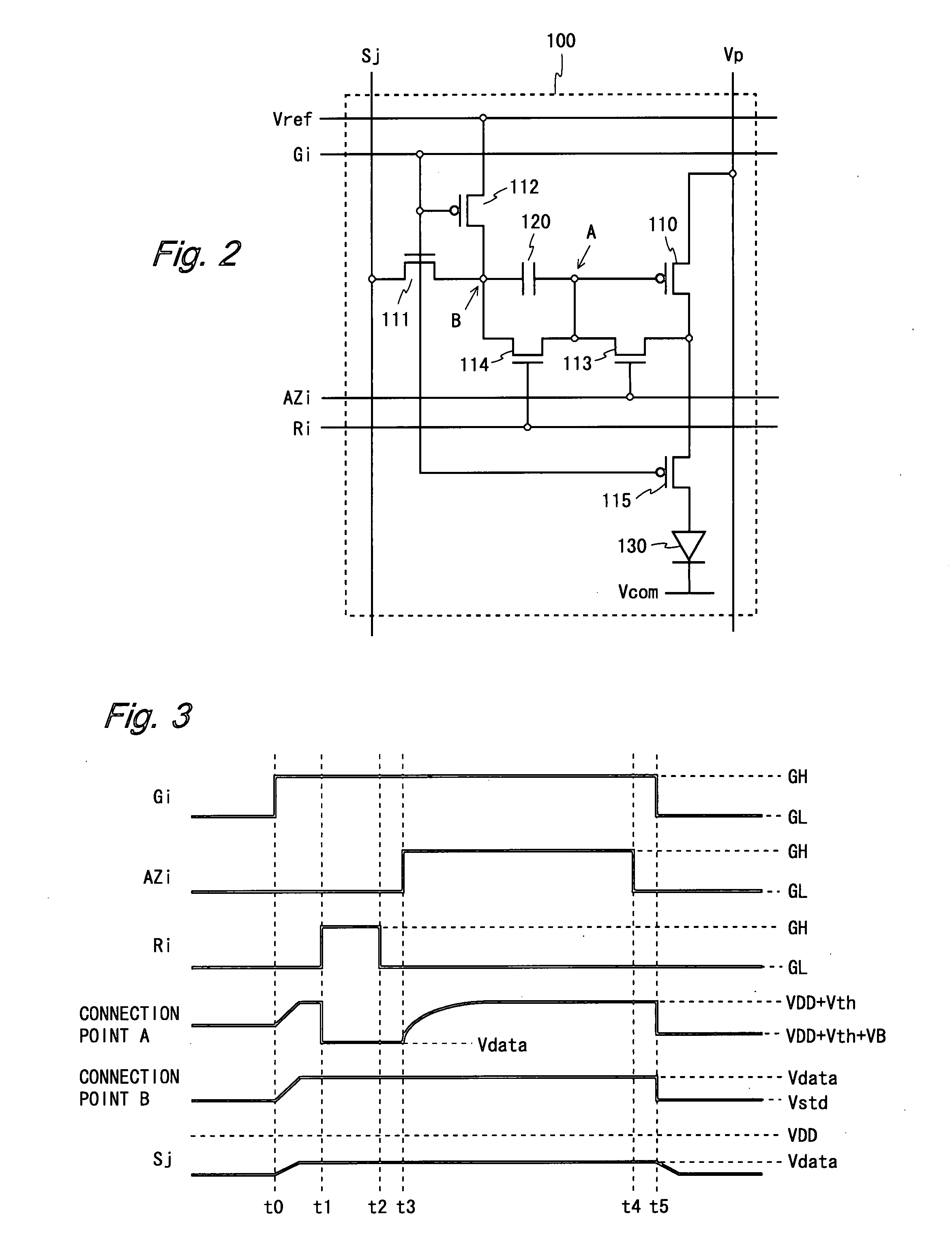
[0071]FIG. 2 is a circuit diagram of a pixel circuit included in a display device according to a first embodiment of the present invention. A pixel circuit 100 shown in FIG. 2 includes a driving TFT 110, switching TFTs 111 to 115, a capacitor 120, and an organic EL element 130. The switching TFTs 111, 113, and 114 are of an n-channel type and other TFTs are of a p-channel type.

[0072]The pixel circuit 100 is connected to a power supply wiring line Vp, a reference supply wiring line Vref, a common cathode Vcom, a scanning line Gi, control lines AZi and Ri, and a data line Sj. Among them, the power supply wiring line Vp (first power supply wiring line) and the common cathode Vcom (second power supply wiring line) are respectively applied with fixed potentials VDD and VSS, and the reference supply wiring line Vref (third power supply wiring line) is applied with a reference potential Vstd. The common cathode Vcom serves as a common electrode for all organic EL elements 130 in the displa...

second embodiment

[0094]FIG. 4 is a circuit diagram of a pixel circuit included in a display device according to a second embodiment of the present invention. A pixel circuit 200 shown in FIG. 4 includes a driving TFT 210, switching TFTs 211 to 215, a capacitor 220, and an organic EL element 230. The switching TFTs 211, 213, and 214 are of an n-channel type and other TFTs are of a p-channel type.

[0095]In a pixel circuit 100 (FIG. 2), a switching TFT 114 is provided between a connection point A and a connection point B. On the other hand, in the pixel circuit 200, the switching TFT 214 is provided between a connection point A and a data line Sj. Except for this point, the configuration of the pixel circuit 200 is the same as that of the pixel circuit 100. As with the pixel circuit 100, the pixel circuit 200 is connected to a power supply wiring line Vp, a reference supply wiring line Vref, a common cathode Vcom, a scanning line Gi, control lines AZi and Ri, and the data line Sj. The same potentials as...

third embodiment

[0097]FIG. 5 is a circuit diagram of a pixel circuit included in a display device according to a third embodiment of the present invention. A pixel circuit 300 shown in FIG. 5 includes a driving TFT 310, switching TFTs 311 to 314, a capacitor 320, and an organic EL element 330. The switching TFTs 311, 313, and 314 are of an n-channel type and other TFTs are of a p-channel type.

[0098]The pixel circuit 300 differs from a pixel circuit 100 (FIG. 2) in the following points. In the pixel circuit 300, a cathode terminal of the organic EL element 330 is connected to a cathode wiring line CAi instead of a common cathode Vcom. The pixel circuit 300 does not include a TFT corresponding to a switching TFT 115, and the driving TFT 310 is directly connected to the organic EL element 330. The potential of the cathode wiring line CAi is individually controlled by a power supply switching circuit (not shown) included in a display device 10. The pixel circuit 300 is connected to a power supply wirin...


PUM


Abstract

In one embodiment of the present invention, to allow a circuit that compensates for variations in a threshold voltage of a drive element to operate properly and prevent luminances of other pixel circuits from fluctuating due to a compensation operation, a pixel circuit is disclosed. A driving TFT, a switching TFT, and an organic EL element are provided between a power supply wiring line and a common cathode, and a capacitor and a switching TFT are provided between a gate terminal of the driving TFT and a data line. A switching TFT is provided between a connection point B between the capacitor and the switching TFT and a reference supply wiring line, a switching TFT is provided between the gate terminal and a drain terminal of the driving TFT, and a switching TFT is provided between the gate terminal of the driving TFT and the connection point B.

Description

TECHNICAL FIELD[0001]The present invention relates to a display device and more particularly to a current-driven display device such as an organic EL display.BACKGROUND ART[0002]In recent years, there has been an increasing demand for thin, lightweight, and fast response display devices. Along with this, research and development for organic EL (Electro Luminescence) displays and FEDs (Field Emission Displays) have been actively conducted. The luminance of an organic EL element included in an organic EL display is substantially proportional to a current flowing through the element and is less susceptible to external factors such as an ambient temperature. Thus, for organic EL displays, it is preferred to apply a current control type drive scheme in which the luminance of an organic EL element is determined by a current value.[0003]Meanwhile, pixel circuits and drive circuits of a display device are made using TFTs (Thin Film Transistors) made of amorphous silicon, low-temperature pol...

Claims


Application Information

Patent Timeline
IPC IPC(8): G09G5/10G09G3/30
CPCG09G3/3233G09G2300/0819G09G1/005G09G2310/0251G09G2310/061G09G2300/0842
Inventor SENDA, TAKAHIRO
Owner SHARP KK
Why Eureka
Try Eureka