Eureka AIR delivers breakthrough ideas for toughest innovation challenges, trusted by R&D personnel around the world.

Semiconductor laser device

Active Publication Date: 2010-05-13
MITSUBISHI ELECTRIC CORP
View PDF3 Cites 0 Cited by
  • Summary
  • Abstract
  • Description
  • Claims
  • Application Information

AI Technical Summary

Benefits of technology

[0005]In recent years, there has been an increasing need to increase the electrical-to-optical power conversion efficiency of semiconductor laser devices in order to reduce the power consumption. The electrical-to-optical power conversion efficiency of a semiconductor laser device can be effectively increased by reducing its threshold current.
[0007]It is, therefore, an object of the present invention to provide an improved semiconductor laser device configured to be able to lase in at least the fundamental, first, and second order modes (i.e., lase in three or more modes), which device has a reduced threshold current and hence an increased electrical-to-optical power conversion efficiency.

Problems solved by technology

However, there is a limit to increasing the optical confinement factor in the waveguide structure of semiconductor laser devices that lase in the fundamental mode in the crystal growth direction.

Method used


Image

  • Semiconductor laser device
  • Semiconductor laser device
  • Semiconductor laser device

Examples


first embodiment

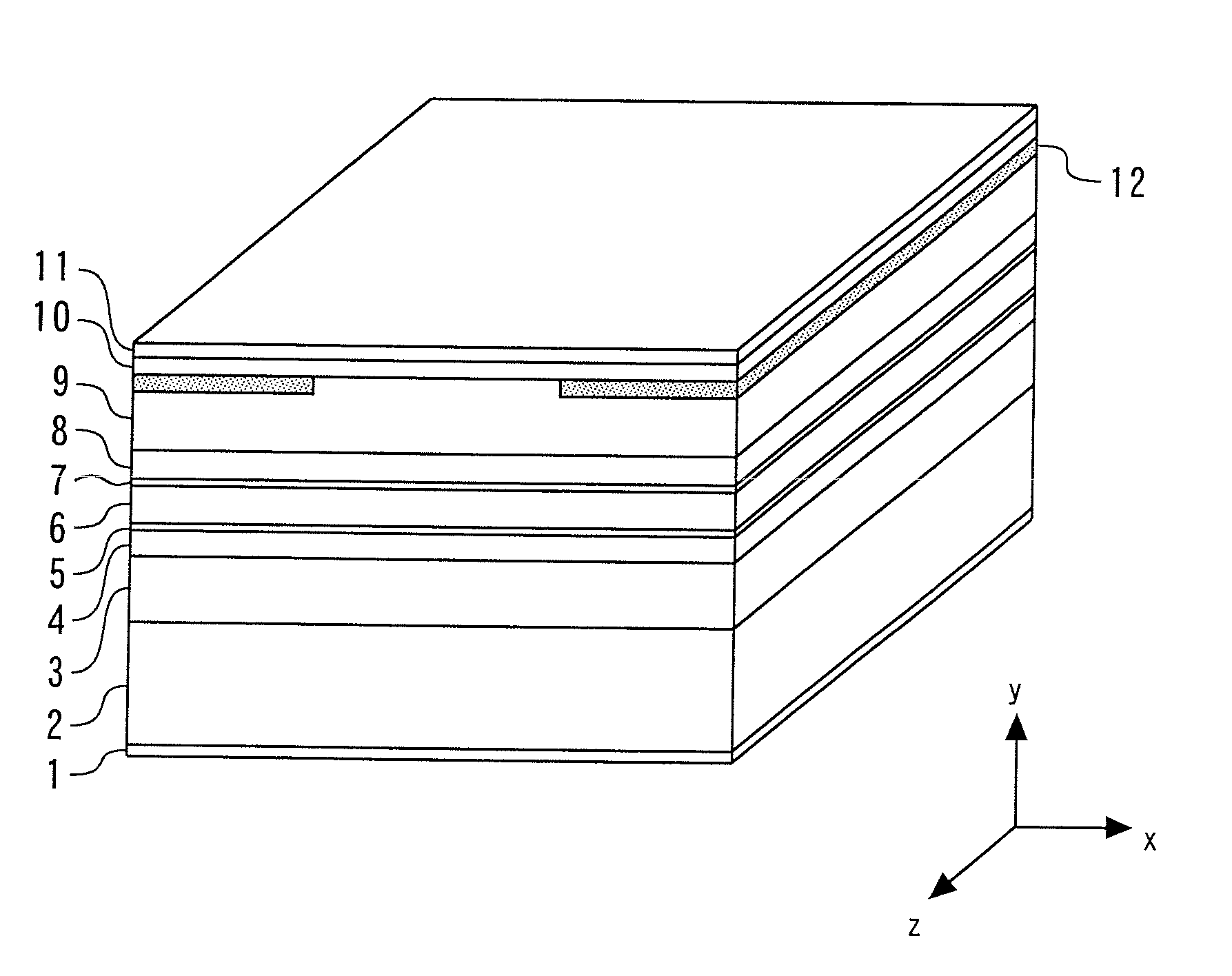
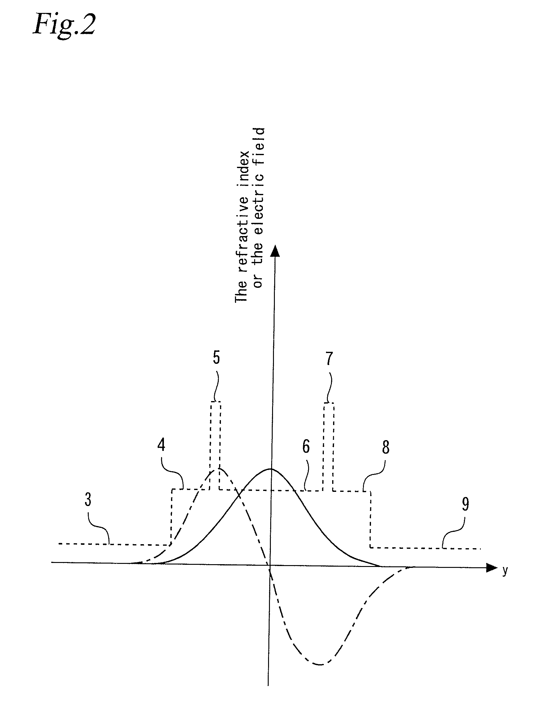
[0021]FIG. 3 is a perspective view of an 810 nm semiconductor laser device according to the first embodiment of the present invention. This semiconductor laser device is configured to lase in modes up to the second order mode, inclusive, and includes three active layers, which are disposed near the locations of extreme points of the electric field of the second order mode.

[Configuration of First Embodiment]

[0022]The configuration of the semiconductor laser device of the present embodiment will be first described with reference to FIG. 3. In FIG. 3, reference numeral 13 denotes an n-side In0.49Ga0.51P guiding layer with a thickness of 100 nm; 14, a GaAs1-xPy active layer with a thickness of 10 nm (where y=0.12); 15, an In0.49Ga0.51P barrier layer with a thickness of 500 nm; 16, a GaAs1-yPy active layer with a thickness of 10 nm (where y=0.12); 17, an In0.49Ga0.51P barrier layer with a thickness of 500 nm; 18, a GaAs1-yPy active layer with a thickness of 10 nm (where y=0.12); and 19, ...

second embodiment

[0028]A second embodiment of the present invention, like the first embodiment, relates to a semiconductor laser device configured to be able to lase in modes up to the second order mode, inclusive. However, this semiconductor laser device differs from that of the first embodiment in the number and the positions of the active layers. More specifically, the semiconductor laser device of the present embodiment includes only two active layers, while that of the first embodiment includes three active layers. In the present embodiment the active layers are respectively disposed near the locations of two extreme points of the electric field of the first order mode, while in the first embodiment the active layers are disposed near the locations of extreme points of the electric field of the second order mode.

[Configuration of Second Embodiment]

[0029]The configuration of the semiconductor laser device of the present embodiment will be first described with reference to FIG. 5. FIG. 5 is a per...


PUM


Abstract

A semiconductor laser device includes: an n-type cladding layer; a p-type cladding layer; and an optical waveguide portion disposed between the n-type and p-type cladding layers and including spaced-apart active layers. The optical waveguide portion permits lasing in a crystal growth direction of the active layers in at least three modes, including the fundamental mode and two higher order modes. The number of active layers is equal to or greater than the number of extreme points of the electric field of a particular one of the higher order modes. At least one of the active layers is disposed near extreme point of the electric field of the particular higher order mode, within the optical waveguide portion.

Description

BACKGROUND OF THE INVENTION[0001]1. Field of the Invention[0002]The present invention relates to a semiconductor laser device.[0003]2. Background Art[0004]Semiconductor laser devices are known which are adapted to lase in the fundamental mode in the crystal growth direction, such as the semiconductor laser device disclosed in J. Sebastian et al., “High-Power 810-nm GaAsP-AlGaAs Diode Lasers With Narrow Beam Divergence,” IEEE J. Select. Topics Quantum Electron., vol. 7, No. 2, pp. 334-339, 2001. In this semiconductor laser device, an active layer is disposed between thick guiding layers having the same thickness. Other prior art includes Japanese Laid-Open Patent Publication Nos. 2001-298241 and 2002-324948.SUMMARY OF THE INVENTION[0005]In recent years, there has been an increasing need to increase the electrical-to-optical power conversion efficiency of semiconductor laser devices in order to reduce the power consumption. The electrical-to-optical power conversion efficiency of a se...

Claims


Application Information

Patent Timeline
IPC IPC(8): H01S5/00
CPCB82Y20/00H01S5/1053H01S5/20H01S2301/18H01S5/343H01S5/3436H01S5/2004
Inventor SHIGIHARA, KIMIO
Owner MITSUBISHI ELECTRIC CORP
Why Eureka
Eureka Blog
Learn More