Organic electroluminescent display device and method of driving the same

a technology of electroluminescent display and organic electroluminescent, which is applied in semiconductor devices, instruments, computing, etc., can solve the problems of thermal degradation of driving tfts “dr, deterioration of brightness uniformity of images on the oeld device, so as to achieve uniform brightness and minimize deviation.

Active Publication Date: 2010-05-20
LG DISPLAY CO LTD
View PDF6 Cites 20 Cited by
  • Summary
  • Abstract
  • Description
  • Claims
  • Application Information

AI Technical Summary

Benefits of technology

[0015]An object of the present invention is to provide an OELD device including driving TFTs having an uniform electric property and being capable of displaying an image having uniform brightness.
[0016]Another object of the present invention is to provide a method of driving an OELD device being capable of minimizing deviation in an electric property of driving TFTs.

Problems solved by technology

Unfortunately, the driving TFT “DR” in each pixel has a deviation in an electric property such that each pixel has different brightness in the same condition.
Accordingly, even if the same voltage is applied to the driving TFT “DR” in each pixel, there are differences in amounts of an electric current passing through the channel of the driving TFT “DR” such that brightness uniformity of images on the OELD device is deteriorated.
On the other hand, in a panel using an amorphous silicon type backplane, there is thermal degradation in the driving TFTs “DR” when the driving TFTs “DR” are driven.
Each driving TFT “DR” in the pixels has a difference in the thermal degradation such that brightness uniformity of images on the OELD device is deteriorated.
As a result, even if each pixel is driven under the same condition, each pixel displays an image having a difference in brightness such that brightness uniformity is deteriorated.

Method used


Image

  • Organic electroluminescent display device and method of driving the same
  • Organic electroluminescent display device and method of driving the same
  • Organic electroluminescent display device and method of driving the same

Examples


first embodiment

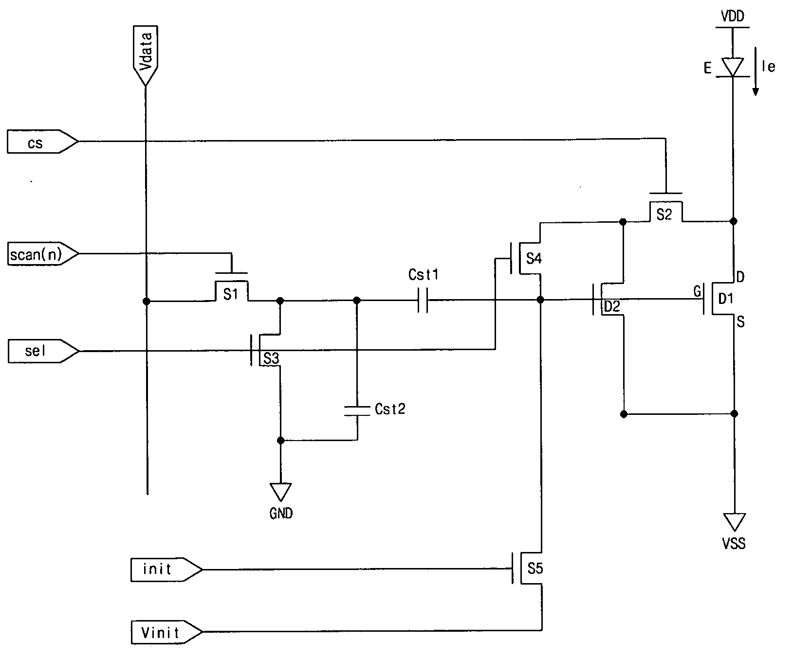
[0041]FIG. 4 is a circuit diagram showing a pixel of an OELD device according to the present invention. In FIG. 4, an OELD includes an organic electroluminescent diode “E”, first to fourth switching TFTs “S1”, “S2”, “S3” and “S4”, first and second driving TFTs “D1” and “D2”, and first and second capacitors “Cst1” and “Cst2” in each pixel. A channel of each of the first to fourth switching TFTs “S1” to “S4” and the first and second driving TFTs “D1” and “D2” may be an NMOS type. Depending on requirements, a channel of each of the first to fourth switching TFTs “S1” to “S4” and the first and second driving TFTs “D1” and “D2” may be a PMOS type.

[0042]The organic electroluminescent diode “E” is connected to a source terminal of the first driving TFT “D1” and a source terminal of the second driving TFT “D2” such that a driving electric current Ie is applied to the organic electroluminescent diode “E”. The first and second driving TFTs “D1” and “D2” have the same properties and are electr...

third embodiment

[0065]FIG. 9 is a timing chart for illustrating a second driving principle of an OELD device according to the present invention. In FIG. 9, a negative voltage is provided in a second frame “{circle around (2)}” after in a first period “{circle around (1)}” which is an emission step in a previous frame. The second frame “{circle around (2)}” may be referred to as a negative voltage applying step “NDI”. The initializing signal “Sinit” is applied to be a high level, while the current providing signal “cs”, the selection signal “sel” and the nth scan signal “scan(n)” are applied to be a low level.

[0066]As a result, the fifth switching TFT “S5” will be switched to be turned on such that the initial voltage “Vinit” of the low level is applied to the gate terminal of the first and second driving TFTs “D1” and “D2” as described below. In this case, the initial voltage “Vinit” is negative such that the threshold voltage (Vth) of the first and second driving TFTs “D1” and “D2”, which is chang...


PUM


Abstract

An organic electroluminescent display device includes an organic electroluminescent diode receiving a driving voltage and a first ground voltage; first and second driving thin film transistors for providing a driving current to the organic electroluminescent diode, each of the first and second driving thin film transistors receiving one of the driving voltage and the first ground voltage; a first switching thin film transistor receiving a data voltage and switched by an nth scan signal to output the data voltage; a second switching thin film transistor switched by a current providing signal to provide the one of the driving voltage and the first ground voltage to the second driving thin film transistor; a third switching thin film transistor receiving a second ground voltage and switched by a selection signal to output the second ground voltage to an output terminal of the first switching thin film transistor; a fourth switching thin film transistor disposed among an output terminal of the second switching thin film transistor, a gate terminal of the first driving thin film transistor and a gate terminal of the second driving thin film transistor and switched by the selection signal; and a first capacitor disposed among the output terminal of the first switching thin film transistor, the gate terminal of the first driving thin film transistor and the gate terminal of the second driving thin film transistor, wherein “n” is a positive integer.

Description

[0001]The present application claims the benefit of Korean Patent Application No. 10-2008-0113712 filed in Korea on Nov. 15, 2008, which is hereby incorporated by reference in their entirety.BACKGROUND OF THE INVENTION[0002]1. Field of the Invention[0003]The present invention relates to an organic electroluminescent display (OELD) device, and more particularly, to an OELD device being capable of displaying an image of uniform brightness and a method of driving the OELD.[0004]2. Background for the Related Art[0005]The liquid crystal display (LCD) device requires a light source therein because it is non-emission type display device. The OELD device is introduced to overcome this disadvantage of an active matrix type liquid crystal display device. In the OELD device, an organic luminescent layer is exited to emit light. The OELD device is driven by a relatively low voltage and has a thin profile.[0006]FIG. 1 is a circuit diagram showing a pixel of an active matrix type OELD device acco...

Claims


Application Information

Patent Timeline
Patent Type & Authority Applications(United States)
IPC IPC(8): G09G5/00G09G3/30
CPCG09G3/3233G09G2300/0819G09G2300/0852G09G2300/0866G09G3/3258G09G2310/0251G09G2310/0262G09G2320/043G09G2300/0876H01L2924/13069
Inventor KIM, SEUNG-TAEBAE, HAE-JINLIM, HO-MINHA, WON-KYUKIM, HAK-SU
Owner LG DISPLAY CO LTD
Why Eureka
Try Eureka