Pattern shape inspection method and apparatus thereof

Inactive Publication Date: 2010-05-20
HITACHI HIGH-TECH CORP
View PDF6 Cites 12 Cited by
  • Summary
  • Abstract
  • Description
  • Claims
  • Application Information

AI Technical Summary

Benefits of technology

[0013]In the present invention, an optical model is formed to indicate a roughness layer formed on a pattern side wall surface corresponding to the edge roughness of the pattern, and to obtain an optical constant of the roughness layer through effective medium approximation. The optical model is used to detect the edge roughness of the pattern based on the spectral waveform of the light reflected from the sample and detected by the first sensor in the first step.
[0014]In the present invention, an

Problems solved by technology

Variation in the size or shape, deficiency and short-circuit of the pattern formed by the optical nano imprinting may cause operatin

Method used


Image

  • Pattern shape inspection method and apparatus thereof
  • Pattern shape inspection method and apparatus thereof
  • Pattern shape inspection method and apparatus thereof

Examples


first embodiment

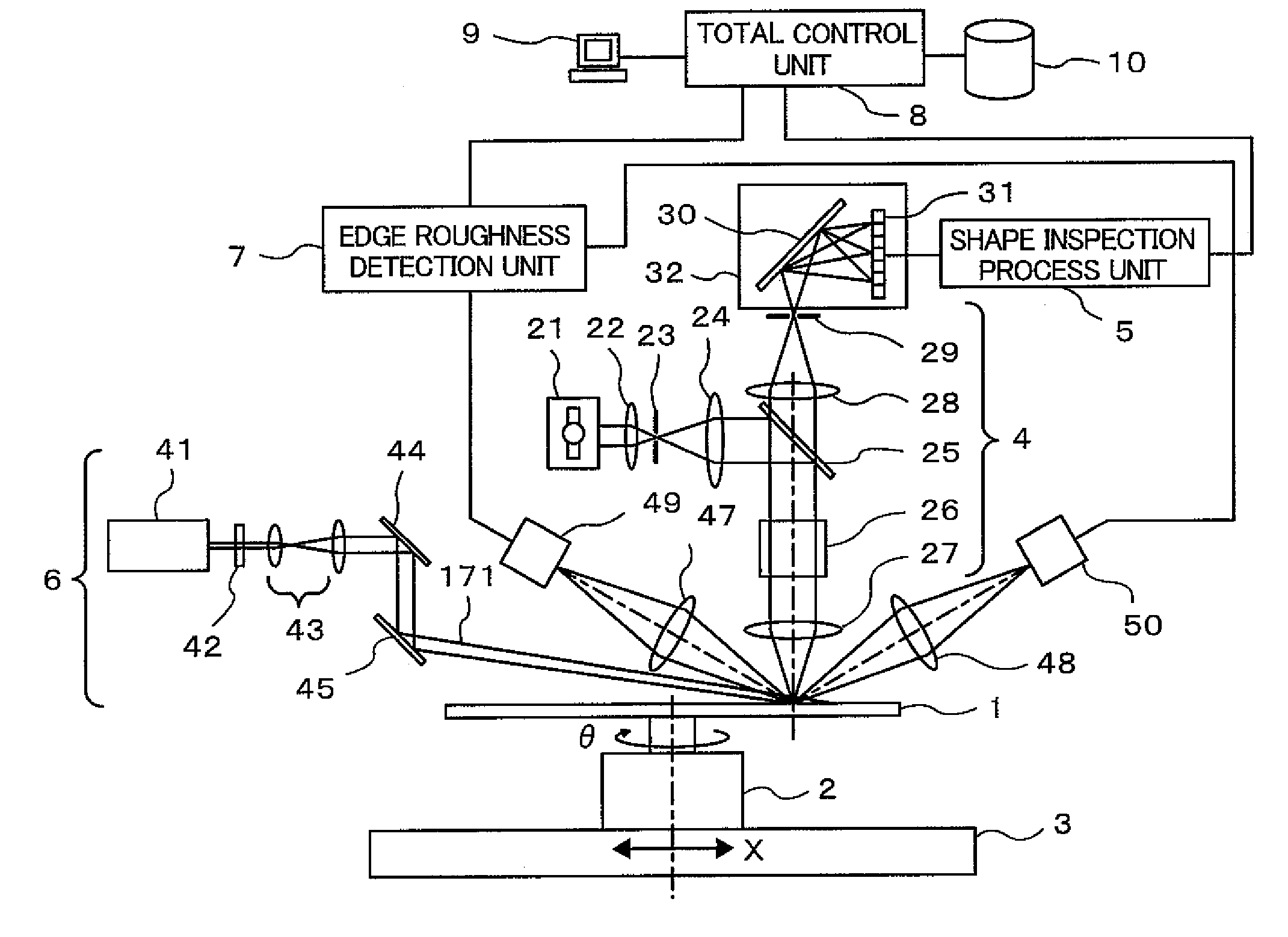
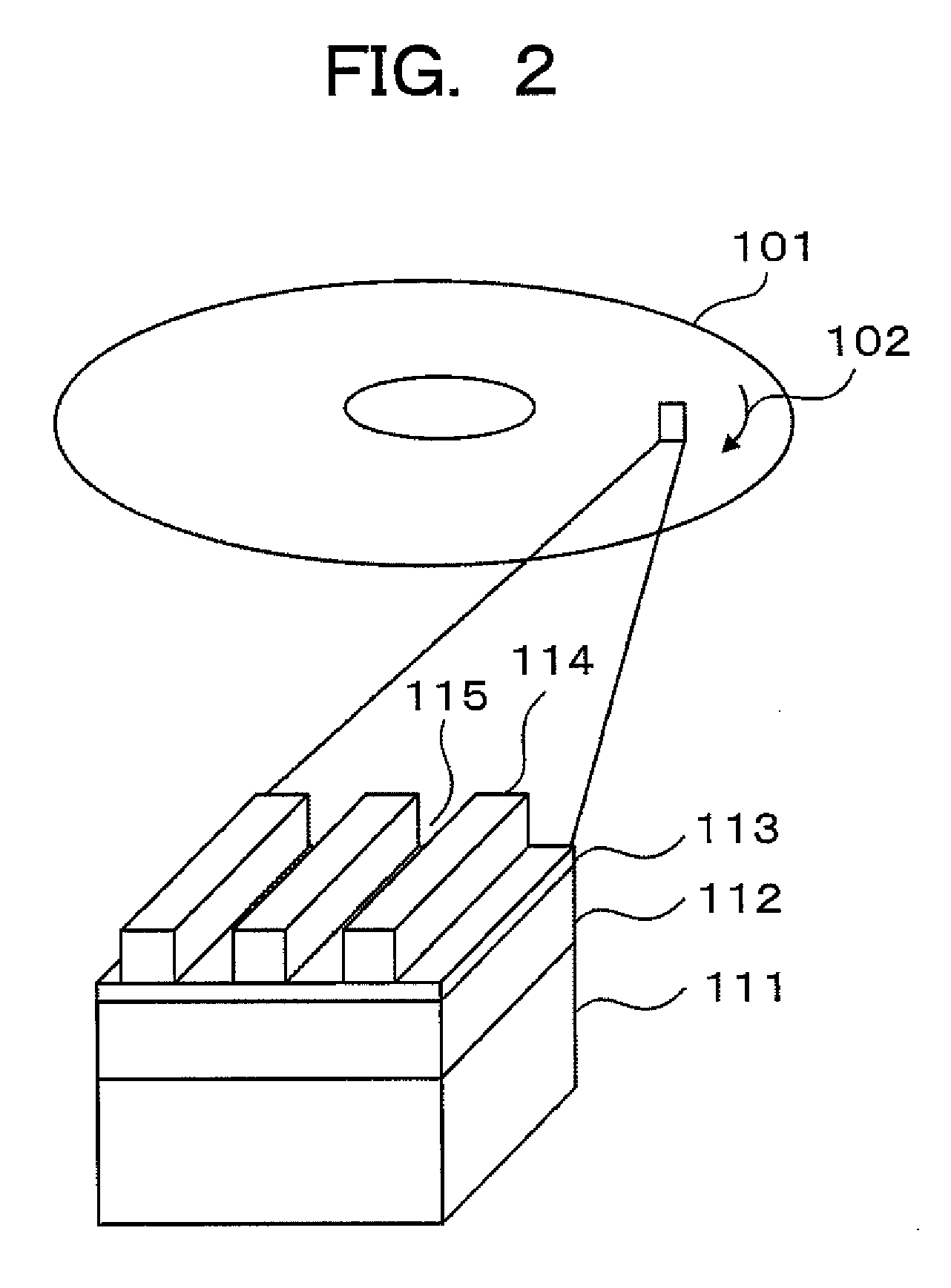
[0036]A first embodiment of the pattern shape inspection apparatus according to the present invention will be described in detail referring to FIGS. 1 to 10. FIG. 1 shows a structure of a pattern shape inspection apparatus according to a first embodiment of the present invention. FIG. 2 shows an inspection object in the form of a discrete track medium as a patterned medium of the magnetic recording medium according to the present invention. The pattern shape inspection apparatus of this invention is used for inspecting (detecting defects of) the pattern shape (for example, track width, height, side wall angle and the like of the track) including a pattern edge state (line edge roughness) of a discrete track medium 101 of a patterned medium for the magnetic recording medium shown in FIG. 2.

[0037]The pattern shape inspection apparatus includes a θ stage 2 which allows a sample 1 in the form of the discrete track medium 101 as the inspection object to be mounted thereon and rotated, an...

second embodiment

[0065]A second embodiment of the pattern shape inspection apparatus according to the present invention will be described referring to FIGS. 5, and 11 to 13. FIG. 5 illustrates the simulated optical model with the pattern edge roughness. FIG. 11 schematically shows the structure of the pattern shape inspection apparatus according to the second embodiment of the present invention.

[0066]Unlike the first embodiment, the second embodiment is not provided with the scattered light detection optical system 6, and the line pattern edge roughness on the patterned medium 101 is detected only by the spectral detection optical system 4.

[0067]The structure of the second embodiment is the same as that of the first embodiment except that the scattered light detection optical system 6 is not provided. The operation of the second embodiment is the same as that of the first embodiment except the process executed by the shape inspection process unit 5.

[0068]The process to be executed by the shape inspe...


PUM


Abstract

This invention relates to a pattern shape inspection method and an apparatus thereof for conducting a first step of irradiating wideband illuminating light which contains far ultraviolet light to a sample from a perpendicular direction, inspecting a shape of the pattern based on a spectral waveform of reflecting light detected from the sample, and detecting an edge roughness of the pattern based on the spectral waveform of the reflecting light detected from the sample, and a second step of irradiating a laser beam to the sample from an oblique direction, and detecting the edge roughness of the pattern based on scattered light detected from the sample.

Description

BACKGROUND[0001]1. Field of the Invention[0002]The present invention relates to a pattern shape inspection method and an apparatus thereof, capable of inspecting a shape of a line pattern on a magnetic recording medium formed of a patterned medium, especially, an inspection object, for example, a discrete track medium, a stamper thereof, or a master as a mold of the stamper as well as a pattern edge state at high speeds with high sensitivity.[0003]2. Description of the Related Art[0004]Recently, a mobile device and AV equipment for digital recording have been rapidly proliferating in addition to the PC and server, and the demand for the use of hard disk drive (HDD) has been growing. Amounts of information processed by the HDD have also been dramatically increasing. Meanwhile, the HDD has been demanded to be compact to increase the recording density of the magnetic recording medium. The perpendicular magnetic recording process has been developed accompanied with the increase in the r...

Claims


Application Information

Patent Timeline
IPC IPC(8): G06K9/00G06V10/60
CPCG06K9/4661G06T2207/10152G06T7/0004G06V10/60
Inventor SAITO, KEIYASASAZAWA, HIDEAKIHIROSE, TAKENORI
Owner HITACHI HIGH-TECH CORP
Why Eureka
Try Eureka