Surface plasmon wavelength converter

a surface plasmon and wavelength converter technology, applied in the field of wavelength converters, can solve the problems of high manufacturing cost of prior art wavelength conversion layers and relatively inefficient

Inactive Publication Date: 2010-05-27
LIGHTWAVE POWER
View PDF3 Cites 84 Cited by
  • Summary
  • Abstract
  • Description
  • Claims
  • Application Information

AI Technical Summary

Benefits of technology

[0023]In one embodiment, the at least one of the centers is disposed within approximately 500 nm or less of at least one of the nanofeatures.
[0024]In another embodi

Problems solved by technology

Such prior art wavelength conversion layers are ex

Method used


Image

  • Surface plasmon wavelength converter
  • Surface plasmon wavelength converter
  • Surface plasmon wavelength converter

Examples


example

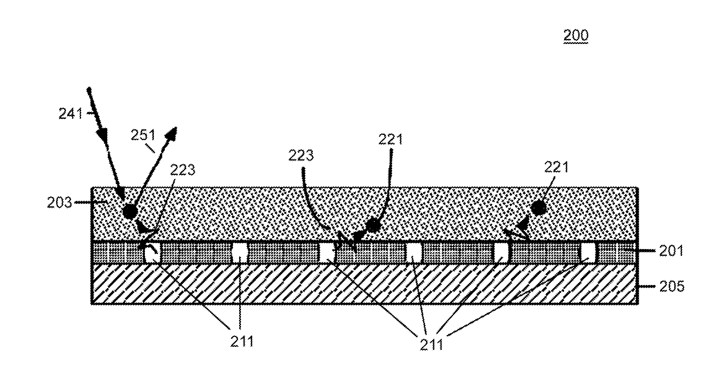
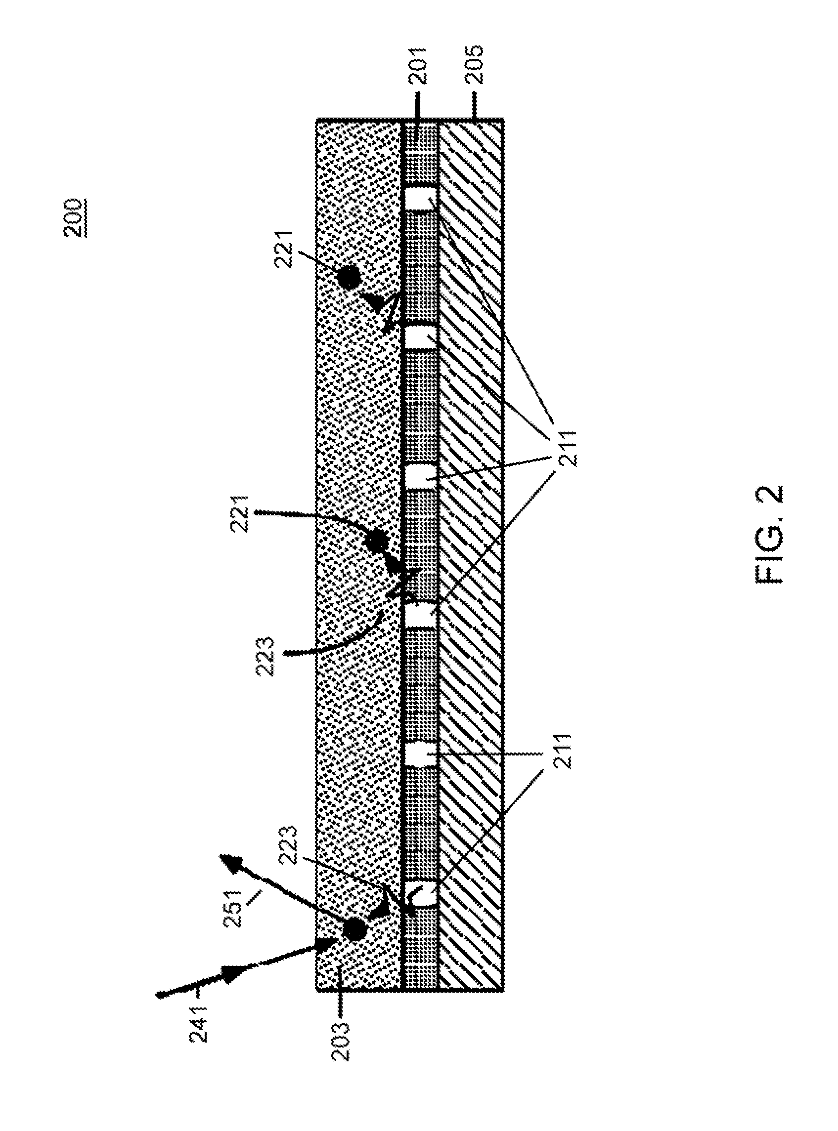
[0089]FIG. 11 shows an illustration of another exemplary embodiment of an integrated solar cell 1100 using stacked layers. Integrated solar cell 1100 includes surface plasmon wavelength converter structure 1110 and surface plasmon wavelength converter structure 1130. Surface plasmon wavelength converter structure 1110 includes a nanofeature layer 1101 having nanofeatures 1111, wavelength conversion layer 1103, and nanofeature layer 1105 having nanofeatures 1141. Surface plasmon wavelength converter structure 1130 includes a nanofeature layer 1131 having nanofeatures 1151, wavelength conversion layer 1133, and nanofeature layer 1135 having nanofeatures 1161. As described hereinabove, nanofeatures 1111, 1141, 1151, and 1161 can include any suitable nanohole pattern including positive and negative patterns such as, triangle, stars, posts, etc. Surface plasmon wavelength converter structure 1110 serves as a downconversion layer at a first surface (e.g. nearer to the front surface of sol...


PUM


Abstract

A surface plasmon wavelength converter device includes a metallic film which has a plurality of nanofeatures. A wavelength conversion layer having a plurality of centers is disposed adjacent to the metallic film. The surface plasmon wavelength converter device is configured to respond to an incident electromagnetic radiation having a first wavelength by radiating away from the surface plasmon wavelength converter device an electromagnetic radiation having a second wavelength. A surface plasmon wavelength converter device having a metallic film and at least one center disposed in at least one of a plurality of nanofeatures of the metallic film is also described. A surface plasmon wavelength converter device having a transparent conductive oxide (TCO) film having a plurality of metallic nanofeatures, adjacent to a wavelength conversion layer, and a TCO film having a plurality of metallic nanofeatures with at least one center disposed therein is also described.

Description

CROSS-REFERENCE TO RELATED APPLICATIONS[0001]This application claims priority to and the benefit of co-pending U.S. provisional patent application Ser. No. 61 / 116,755, PERIODIC OR NON-PERIODIC NANOSTRUCTURES TO CONTROL EMISSION ENVIRONMENT FOR ENHANCED WAVELENGTH SHIFTING EFFICIENCY, filed Nov. 21, 2008, which application is incorporated herein by reference in its entirety. This application is also related to co-pending PCT Application No. PCT / U.S.09 / 36815, entitled INTEGRATED SOLAR CELL WITH WAVELENGTH CONVERSION LAYERS AND LIGHT GUIDING AND CONCENTRATING LAYERS, filed Mar. 11, 2009, which is incorporated by reference in its entirety.FIELD OF THE INVENTION[0002]The invention relates to wavelength converter in general and particularly to a surface plasmon wavelength converter.BACKGROUND OF THE INVENTION[0003]FIG. 1 shows an illustration of a solar cell according to the prior art. A solar cell 100 is typically made from single crystal silicon. The solar cell 100 has a PN junction 101...

Claims


Application Information

Patent Timeline
IPC IPC(8): G02F1/35H01L31/02
CPCG02B5/008G02F2/02G02F2202/36Y02E10/52H01L31/02322H01L31/055G02F2203/10
Inventor JI, JIN
Owner LIGHTWAVE POWER
Why Eureka
Try Eureka