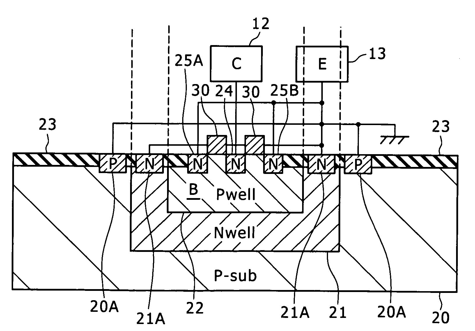
[0025]In the first and second modes, the common anode of the two diodes forms a floating node. Therefore, if the voltage applied to the protection element increases steeply due, for example, to the application of a surge, the potential of the common anode will also increase steeply, turning ON one of the diodes depending on the potential of the location to which the common anode is connected. This turns ON an NPN-type parasitic bipolar transistor, steeply reducing the impedance of the protection element from this moment onward and rapidly eliminating the surge.
Problems solved by technology
However, it has a high trigger voltage, making it difficult to adjust the trigger voltage.
As a result, using a thyristor in an internal circuit with a low withstand voltage may damage the internal circuit before the thyristor turns ON.
GGMOS and unidirectional diode protection elements are not applicable, for example, to a signal line or the like whose signal potential could conceivably exceed the VDD potential or fall below the VSS potential due to a significant fluctuation of the signal DC level.
This results in distortion of the signal having such a waveform.
Further, a GGMOS protection element may not track a high-frequency signal input because of its large parasitic capacitance, resulting in attenuation of the signal.
Method used
Image
Click on the blue label to locate the original text in one second.
Reading with bidirectional positioning of images and text.
Examples
modification examples
7. Modification examples
8. Comparative examples and effects of the embodiments
first embodiment
1. First Embodiment
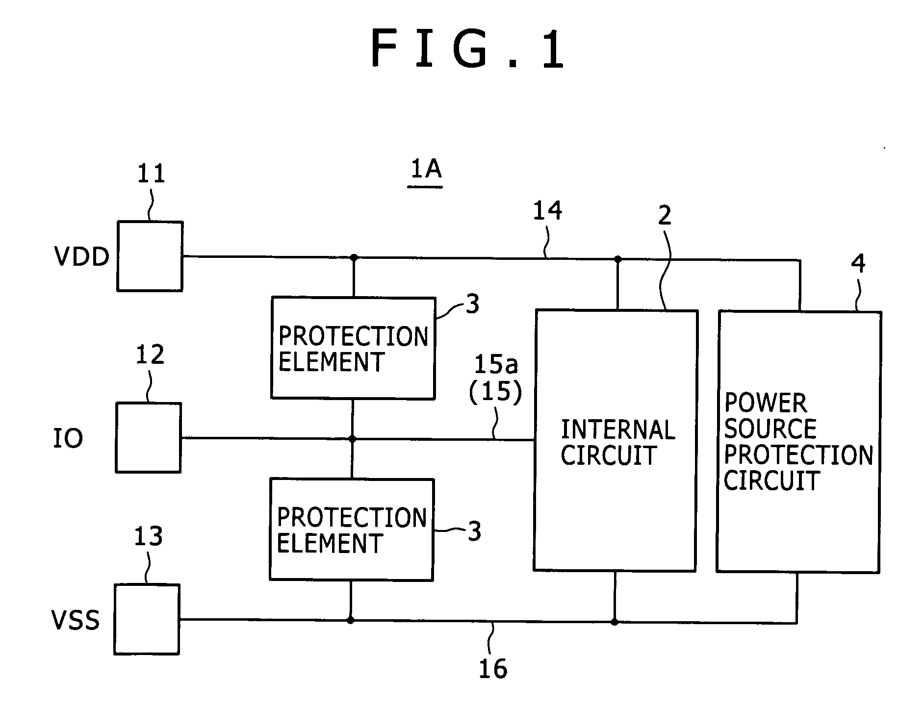
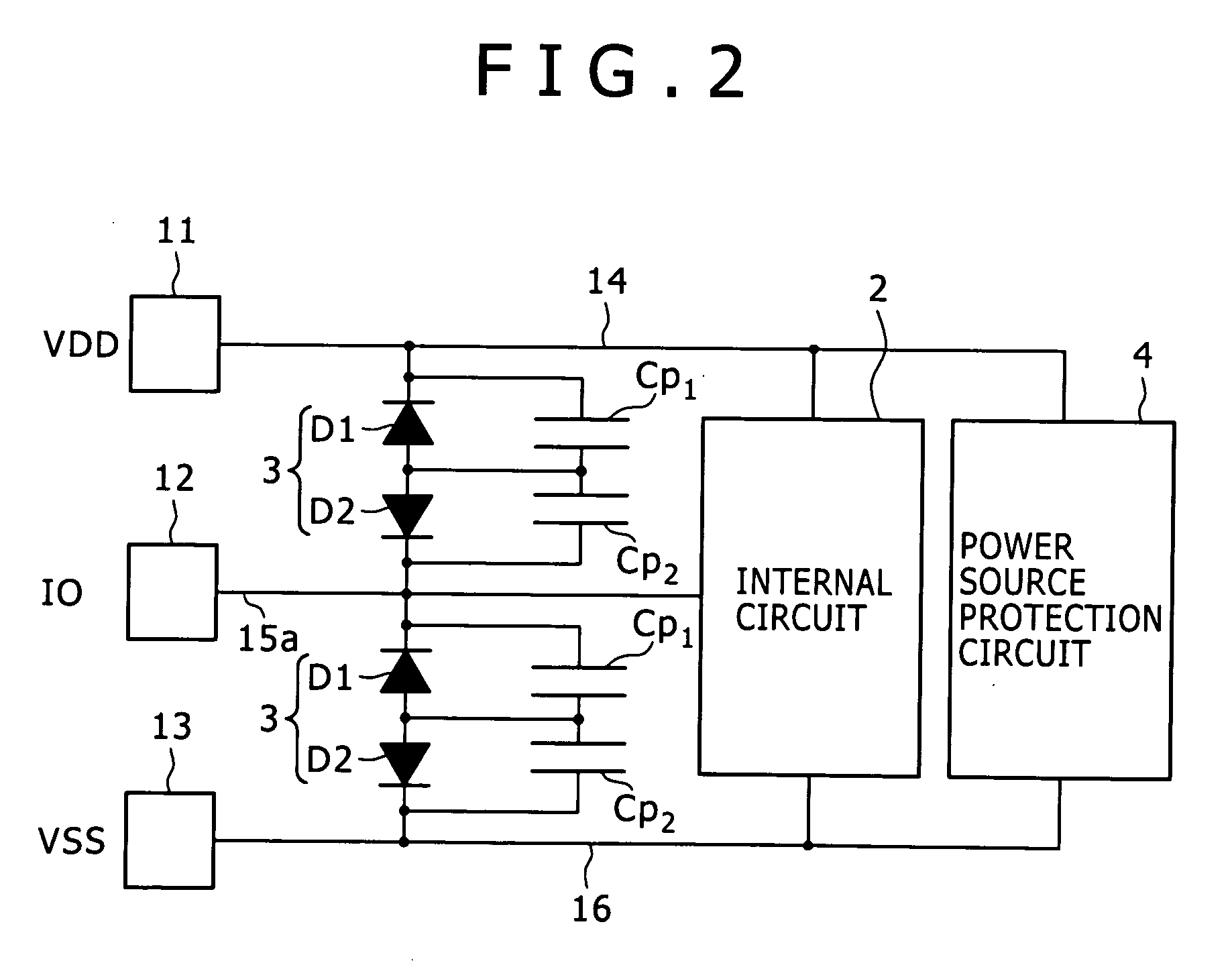
[0049]FIG. 1 is a configuration diagram of main components of a semiconductor integrated circuit according to a first embodiment. FIG. 2 illustrates the protection element represented by an equivalent circuit in the configuration diagram of FIG. 1.
[0050]A semiconductor integrated circuit 1A shown in FIG. 1 includes an internal circuit 2 serving as a “protected circuit” and three terminals electrically connected to the internal circuit 2.
[0051]Here, the three terminals are a supply terminal of the source voltage VDD (VDD terminal 11), IO terminal 12 and a supply terminal of the reference voltage VSS (VSS terminal 13).
[0052]The source voltage VDD has a positive level of, for example, 1 to 5 V. The same voltage VDD is supplied, for example, from a source external to the semiconductor integrated circuit 1A. The same voltage VDD is applied from the VDD terminal 11 to the internal circuit 2 via the VDD line 14.
[0053]The reference voltage VSS is, for example, a 0 V groun...
second embodiment
2. Second Embodiment
[0076]FIG. 3 illustrates main components of a semiconductor integrated circuit according to a second embodiment.
[0077]As in FIG. 1, a semiconductor integrated circuit 1B shown in FIG. 3 includes the internal circuit 2 serving as a “protected circuit,” power source protection circuit 4, VDD terminal 11, 10 terminal 12, VSS terminal 13, VDD line 14, wiring 15 (e.g., signal input line 15a) and VSS line 16. Here, the power source protection circuit 4 is an arbitrary component in the first embodiment. However, the same circuit 4 is desired in the second embodiment to ensure more complete protection.
[0078]The semiconductor integrated circuit 1B shown in FIG. 3 differs from the semiconductor integrated circuit 1A shown in FIG. 1 in that the protection element 3 is connected between the wiring 15 and VSS line 16, but none between the wiring 15 and VDD line 14.
[0079]The semiconductor integrated circuit 1B is identical to the semiconductor integrated circuit 1A in all othe...
PUM
Abstract
Disclosed herein is a semiconductorintegrated circuit including a protected circuit; and a protection element formed on the same semiconductor substrate as the protected circuit and adapted to protect the protected circuit, wherein the protection element includes two diodes having their anodes connected together to form a floating node and two cathodes connected to the protected circuit, the two diodes are formed in a well-in-well structure on the semiconductor substrate, and the well-in-well structure includes a P-type well forming the floating gate, an N-type well which surrounds the surfaces of the P-type well other than that on the front side of the substrate with the deep portion side of the substrate so as to form the cathode of one of the diodes, and a first N-type region formed in the P-type well so as to form the cathode of the other diode.
Description
BACKGROUND OF THE INVENTION[0001]1. Field of the Invention[0002]The present invention relates to a semiconductor integrated circuit having a protection element which is connected to an element or circuit to be protected (protected circuit) so as to remove input noise.[0003]2. Description of the Related Art[0004]Some semiconductor integrated circuits have a protection element adapted to perform electrostatic discharge (ESD) so as to protect the internal circuit from static electricity which finds its way into the circuit from an external terminal.[0005]An ESD protection element is connected between two wirings connected to the internal circuit. One of such wirings is, for example, a supply line (hereinafter VDD line) of a source voltage VDD or a supply line (hereinafter VSS line) of a reference voltage VSS (e.g., GND voltage). The other of such wirings is, for example, a signal line. On the other hand, a power line discharge element (a type of ESD protection element) may be connected...
Claims
Application Information
Patent Timeline
Application Date:The date an application was filed.
Publication Date:The date a patent or application was officially published.
First Publication Date:The earliest publication date of a patent with the same application number.
Issue Date:Publication date of the patent grant document.
PCT Entry Date:The Entry date of PCT National Phase.
Estimated Expiry Date:The statutory expiry date of a patent right according to the Patent Law, and it is the longest term of protection that the patent right can achieve without the termination of the patent right due to other reasons(Term extension factor has been taken into account ).
Invalid Date:Actual expiry date is based on effective date or publication date of legal transaction data of invalid patent.

