Method for stacking and interconnecting integrated circuits

Active Publication Date: 2010-06-03
STMICROELECTRONICS SRL
View PDF7 Cites 18 Cited by
  • Summary
  • Abstract
  • Description
  • Claims
  • Application Information

AI Technical Summary

Problems solved by technology

The interconnection of integrated circuits has become more and more complex with the increasing complexity of the integrated circuits.
However, various technological constraints prevented the rapid implementation of such a solution.
These methods are not very practical to implement when several wafers are stacked.
After a step of alignment of the different wafers, the bonding and interconnection of the wafers is a delicate operation due t

Method used


Image

  • Method for stacking and interconnecting integrated circuits
  • Method for stacking and interconnecting integrated circuits
  • Method for stacking and interconnecting integrated circuits

Examples


first embodiment

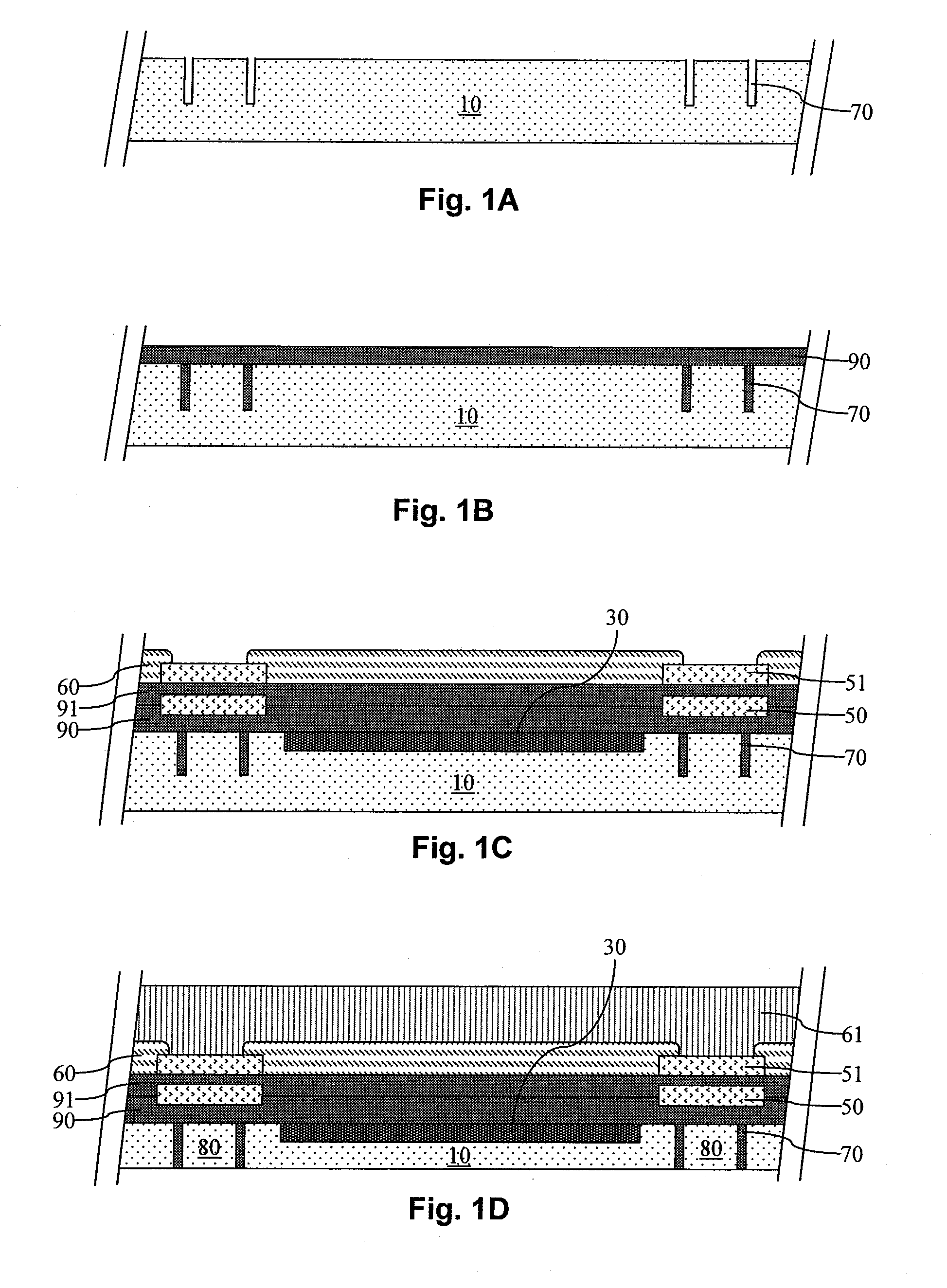
[0037]FIGS. 1A to 1H show different steps of a method for stacking and interconnecting integrated circuits according to the disclosure. The method is implemented by means of wafers in which several integrated circuits are realized. For the sake of simplicity, only partial areas of the wafers are shown. These zones correspond to a region of a wafer comprising an integrated circuit. For reasons of clarity, the drawings are not to scale and are stretched in the vertical axis corresponding to the thickness of the wafers.

[0038]The method comprises a preliminary step of forming recesses on the front face of a wafer 10, as shown in FIG. 1A. In FIG. 1A, the recesses are trenches 70, although other types of recesses could be formed. This preliminary step may comprise steps of deposition of a photoresist layer, exposure of the photoresist with a photomask, development of the photoresist to obtain windows in the photoresist, etching of the wafer within the windows in the photoresist, removal o...

second embodiment

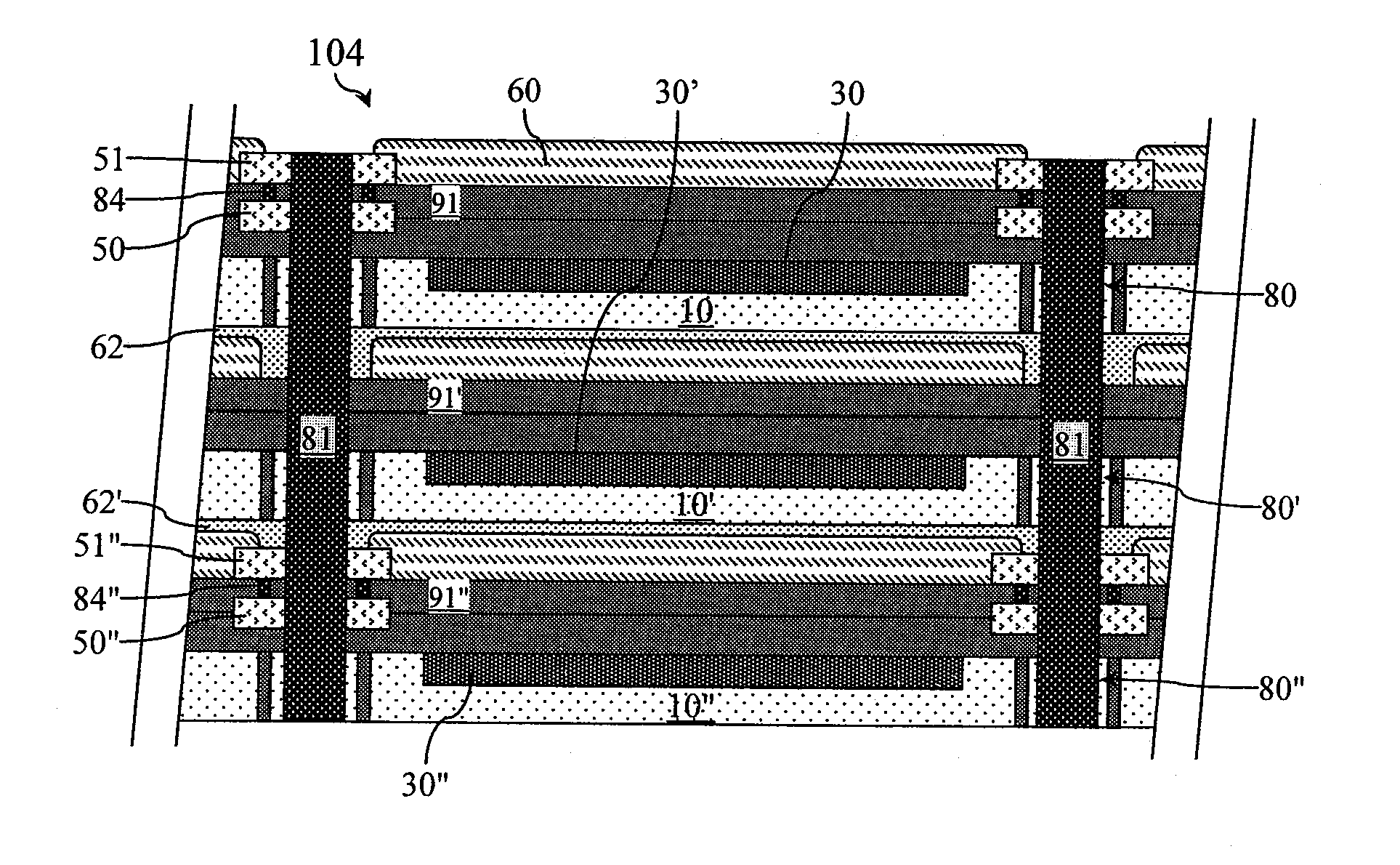
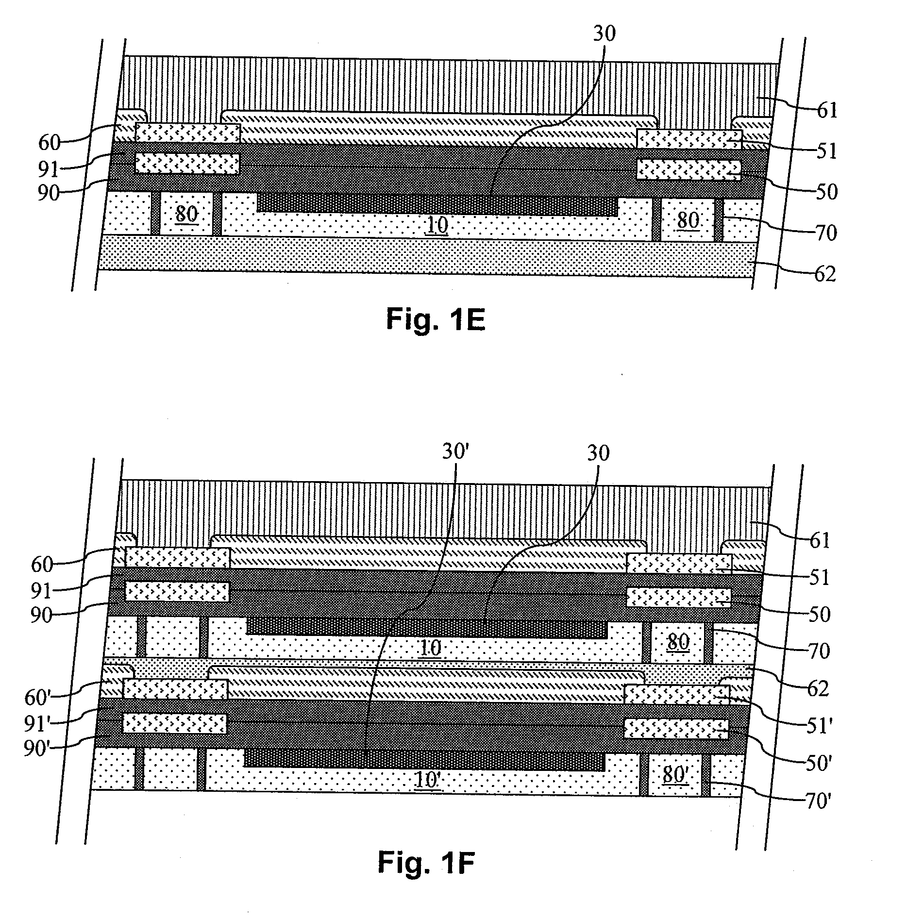
[0058]FIGS. 3A and 3B show a wafer stack 101 made according to the method of the disclosure. As previously indicated, only an area of each wafer comprising a single integrated circuit is shown.

[0059]In this embodiment, three wafers 10, 10′, 10″ have been fabricated, bonded and interconnected by conductive columns 81 such as in the manner described above. Then, as shown in FIG. 3A, the conductive material is removed in top parts of the conductive columns 81, for example by etching, to a depth D1. A hole 72 is thus obtained. The depth D1 of the hole is chosen so that the contact pads 51 on the front face of the top wafer 10 are no longer connected to the other contact pads that are in contact with the conductive columns. The hole 72 is then filled with a material 82, such as an insulating material, as shown in FIG. 3B.

[0060]This embodiment can be implemented for various reasons, for example to block the electrical connections between on one hand the contact pads on the front face of t...

third embodiment

[0061]FIG. 4 shows a wafer stack 102 in accordance with the method of the disclosure.

[0062]In this embodiment, two wafers 10, 10′ have been fabricated and bonded as described above. A first hole has been formed completely through wafers 10, 10′ and filled with a conductive material so as to create a first conductive column 81a that interconnects vertically-aligned contact pads 50a, 51a of wafer 10 and 50a′, 51a′ of wafer 10′. A third wafer 10″ was then bonded to wafers 10, 10′ to obtain a stack of wafers 10, 10′, 10″. A second hole was then formed, completely traversing the wafer stack and filled with a conductive material so as to create a second conductive column 81b that interconnects vertically-aligned contact pads 50b, 51b of wafer 10, 50b′, 51b′ of wafer 10′ and 50b″, 51b″ of wafer 10″.

[0063]Additionally, when the wafer 10″ was processed to create the contact pads 50a″, 51a″, conventional conductive vias 84″ were fabricated to interconnect the contact pads 50a″, 51a″, for exam...


PUM


Abstract

A method for stacking and interconnecting integrated circuits includes providing at least two substrates; forming a trench in each substrate; filling the trench with an insulating material; forming, in each substrate, at least one conductive area; thinning each substrate until reaching at least the bottom of the trench, to obtain in each substrate at least one electrically insulated region within the closed perimeter delineated by the trench; bonding the substrates together; making at least one hole through the bonded substrates so that the hole passes at least partially through the conductive areas and passes through the insulated region of each substrate; and filling the hole with an electrically conductive material so as to obtain a conductive column that traverses the isolated region of each substrate and is in lateral electrical contact with the conductive areas.

Description

BACKGROUND[0001]1. Technical Field[0002]The present disclosure relates to the manufacture of integrated circuits and more particularly to the manufacture of a stack of integrated circuit chips.[0003]2. Description of the Related Art[0004]The interconnection of integrated circuits has become more and more complex with the increasing complexity of the integrated circuits. In order to minimize as much as possible the area necessary to interconnect integrated circuits, it is generally necessary to provide interconnection means such as chip carriers or high-density integrated circuit cards.[0005]For years, the realization techniques of three-dimensional integrated circuits have been seen as the ideal solution to reduce the surface occupied by an ensemble of interconnected integrated circuits. However, various technological constraints prevented the rapid implementation of such a solution.[0006]Conventionally, a three-dimensional integrated circuit is a stack of two or more semiconductor ...

Claims


Application Information

Patent Timeline
IPC IPC(8): H01L29/06H01L21/98
CPCH01L21/76898H01L23/481H01L25/0657H01L25/50H01L2225/06513H01L2224/48091H01L2225/06541H01L2224/16H01L2924/00014
Inventor DUNNE, BRENDAN
Owner STMICROELECTRONICS SRL
Why Eureka
Try Eureka