Switching power supply control circuit

a control circuit and power supply technology, applied in the direction of electric variable regulation, process and machine control, instruments, etc., can solve the problems of system sometimes not being able to bring into operation in a normal mode, light emitting element coupler pcb>2/b> cannot be turned on, so as to avoid the disadvantage of the related switching power supply control circuit

Active Publication Date: 2010-06-03
FUJI ELECTRIC CO LTD
View PDF6 Cites 36 Cited by
  • Summary
  • Abstract
  • Description
  • Claims
  • Application Information

AI Technical Summary

Benefits of technology

[0026]With the disclosed switching power supply control circuit according to the invention, the disadvantage in the related switching power supply control circuit can be avoided in that the switching power supply control circuit makes an erroneous decision that the switching power supply circuit is in a stand-by mode before an increase in an output voltage at the starting up of the power supply to make the switching power supply circuit impossible to return into a normal mode. As a result, it becomes possible that the switching power supply system can be made to start up stably in an instructed mode at the turning-on of the power supply.

Problems solved by technology

In the related switching power supply system, however, there was a problem that the system sometimes can not be brought into operation in a normal mode after being made to start up in either one of the two kinds of modes.
However, the low output voltage of the second converter 20 makes the light emitting element 25 in the photo coupler PC2 impossible to be turned-on.
Therefore, no sufficient energy (current) can be supplied onto the output side of the second converter 20.
Thus, there is a problem in that presence of a load being heavy to some extent from the beginning as in the rated load starting up mode makes at turning-on of the power supply the switching power supply circuit caught in a vicious cycle of causing no output voltage to be increased, enabling next no photo coupler to be turned-on, making then the switching power supply circuit brought in no normal operation mode (no rated load condition) and thus causing no output voltage to be increased.
Thus, the charges in an output capacitor are consumed in the turned-on photo couplers, which consumption gradually reduces the output voltage.
This makes it impossible for the switching power supply circuit to maintain the state in the stand-by mode for a long time.
Thus, there is a possibility of making a photo coupler impossible to be forced to emit light to make the switching power supply circuit impossible to maintain a state in the stand-by mode or impossible to drive a load when the stand-by mode is cancelled.
The same problem arises even though a switching power supply system is one formed of one converter (such as a flyback power supply, for example) rather than one formed of two stage converters as shown in FIG. 6.
That is, in the case where the converter is one that carries out a stop of its switching operation, an intermittent operation or PFM control at a low frequency when in a stand-by state, since the output current of the converter is limited in a stand-by mode, when a load current is larger than the current which can be supplied by the converter once brought into the stand-by mode at the start up in a rated load start up mode, the same defect as above is caused.

Method used


Image

  • Switching power supply control circuit
  • Switching power supply control circuit
  • Switching power supply control circuit

Examples


first embodiment

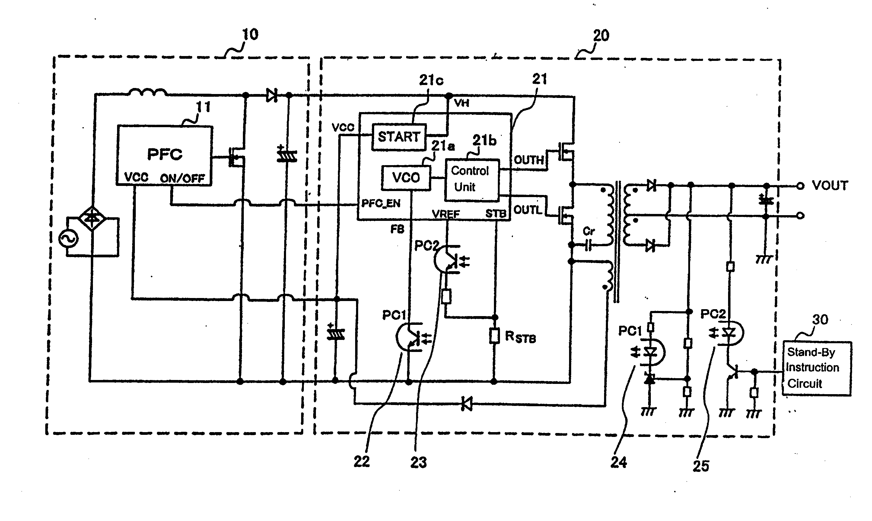
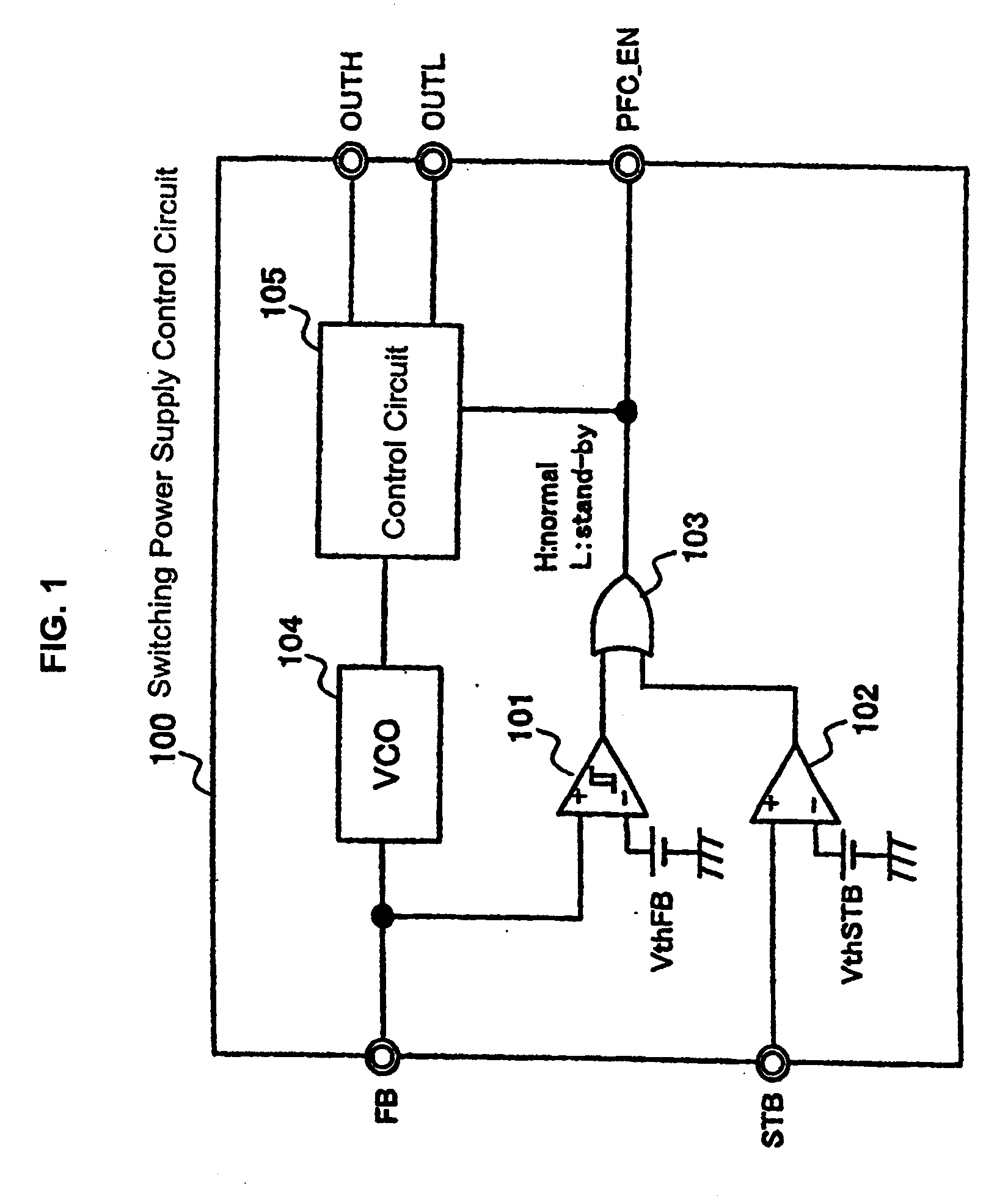
[0038]FIG. 1 is a circuit diagram showing a switching power supply control circuit according to the invention. The switching power supply control circuit 100 is included in, for example, the control IC 21 shown in FIG. 6 to form the control IC 21.

[0039]The switching power supply control circuit 100 has a first comparator 101 (hereinafter referred to as “comparator 101”), a second comparator 102 (hereinafter referred to as “comparator 102”), a decision circuit 103, a VCO 104 and a control circuit 105. Double circles in FIG. 1 represent input terminals and output terminals. An FB terminal, an STB terminal, an OUTH terminal, an OUTL terminal and a PFC EN terminal are terminals for inputting a feedback signal of an output voltage detection signal (hereinafter simply referred to as “feedback signal”), for inputting an instruction input signal instructing an operation mode, for outputting a high level output signal, for outputting a low level output signal and for outputting an inner stan...

second embodiment

[0061]FIG. 5 is a circuit diagram showing a switching power supply control circuit according to the invention. The switching power supply control circuit 110 is also included in, for example, the control IC 21 shown in FIG. 6 to form the control IC 21. The same constituents as those of the switching power supply control circuit 100 shown in FIG. 1 are denoted by the same reference numerals and signs.

[0062]The switching power supply control circuit 110 is a circuit additionally having a third comparator 112 (hereinafter referred to as “comparator 112”) and a flip-flop circuit (hereinafter referred to as “FF”) 113 to the switching power supply control circuit 100 with a comparator 111 placed instead of the comparator 101.

[0063]Here, the comparator 111, like the comparator 101 in the switching power supply control circuit 100, has an FB terminal voltage and a threshold voltage VthFB inputted to its two input terminals, respectively, to compare the values of the two voltages. However, t...


PUM


Abstract

A comparator detects whether a feedback signal of an output voltage detecting circuit for a switching power supply circuit reaches a control voltage. A comparator detects an operating state of the switching power supply circuit, which is instructed by a switching instruction signal, by comparing the instruction signal with a reference voltage. The comparators are connected to a decision circuit which outputs to a control circuit a signal instructing a normal state until the feedback signal reaches the control voltage, and thereafter a signal instructing a normal state or a stand-by state that is instructed by the switching instruction signal. Thus, the control circuit makes the switching power supply circuit operate in a normal state until the output voltage reaches the control voltage. After the output voltage reaches the control voltage, the switching power supply circuit operated in an operation state instructed by the switching instruction signal to enable stable startup.

Description

BACKGROUND OF THE INVENTION[0001]The present invention relates to a switching power supply control circuit and more particularly to a switching power supply control circuit that operates a switching power supply system by switching its state between a normal state and a stand-by state.[0002]At present, a switching power supply system that supplies power to various kinds of electric devices generally supplies power in two modes, a normal mode in which electric devices as objects of supplying electric power are made to carry out normal operations and a stand-by mode in which the electric devices are brought into stand-by states.[0003]FIG. 6 is a circuit diagram showing an example of a switching power supply circuit forming a switching power supply system. The switching power supply circuit of the example shown in FIG. 6 is formed of two stages of a first converter 10 and a second converter 20. The first converter 10 is a PFC (Power Factor Control) step-up converter in which a PFC circ...

Claims


Application Information

Patent Timeline
Patent Type & Authority Applications(United States)
IPC IPC(8): H02M3/337G05F1/46H02M7/217
CPCH02M1/36H02M1/4225Y02B70/16Y02B70/126H02M2001/0032Y02B70/10H02M1/0032
Inventor SONOBE, KOJI
Owner FUJI ELECTRIC CO LTD
Why Eureka
Try Eureka