
Self-aligned multi-patterning for advanced critical dimension contacts

Active Publication Date: 2010-06-03
APPLIED MATERIALS INC
View PDF1 Cites 27 Cited by
  • Summary
  • Abstract
  • Description
  • Claims
  • Application Information

AI Technical Summary

Benefits of technology

[0005]Embodiments of the present invention pertain to methods of forming patterned features on a substrate having a reduced pitch in two dimensions as compared to what is possible using standard photolithography processing techniques using a single high-resolution photomask. A spacer layer is formed over a two-dimensional square grid of cores with a thickness chosen to leave a dimpl

Problems solved by technology

Clearly, the minimum pitch of any given photolithographic technique can limit feature size reduction.

Method used


Image

  • Self-aligned multi-patterning for advanced critical dimension contacts
  • Self-aligned multi-patterning for advanced critical dimension contacts
  • Self-aligned multi-patterning for advanced critical dimension contacts

Examples


Embodiment Construction

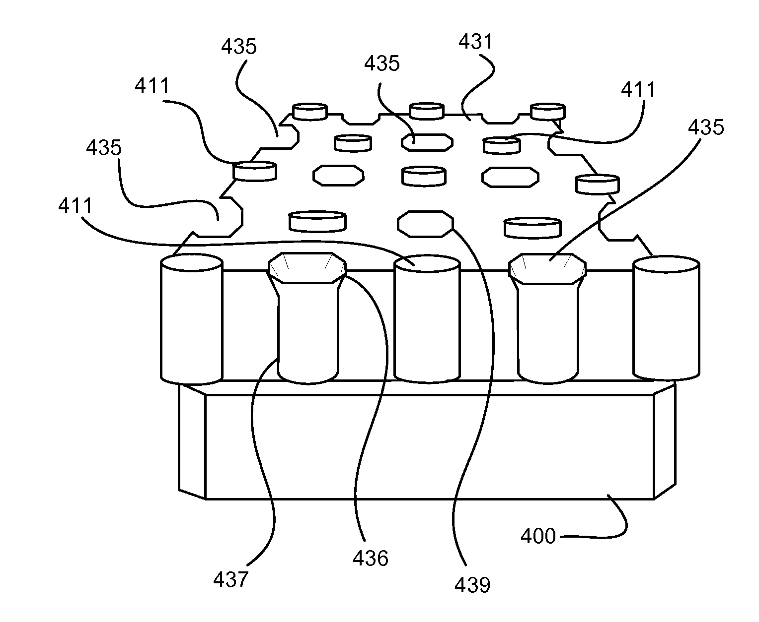
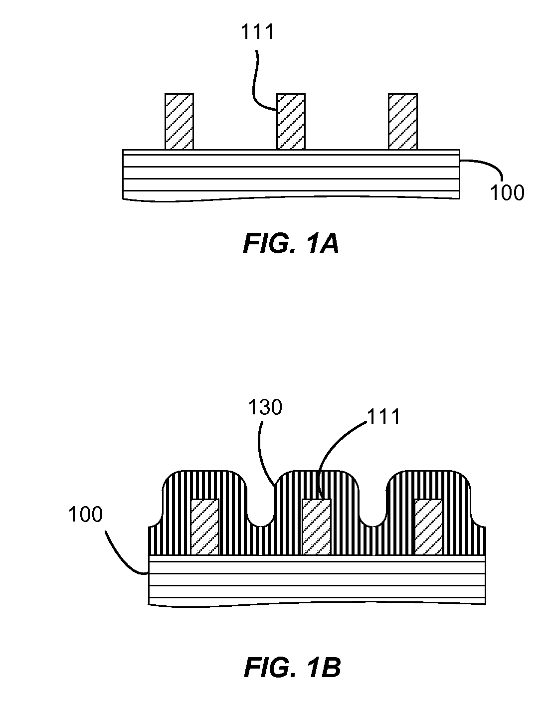
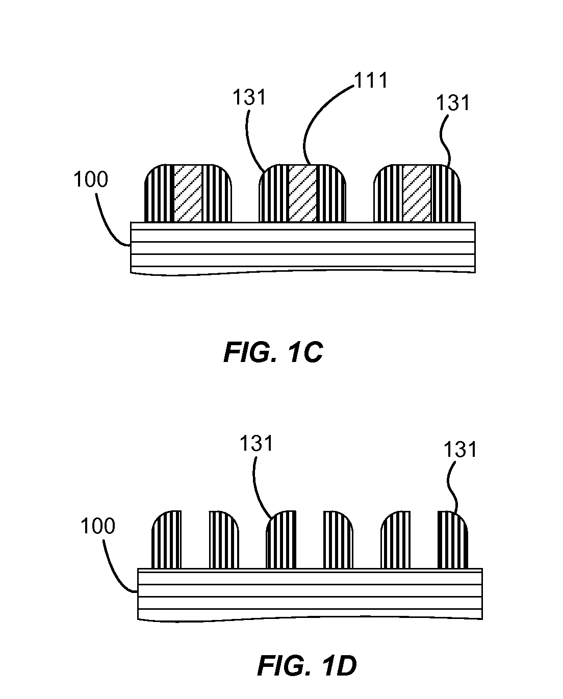
[0015]Embodiments of the present invention pertain to methods of forming patterned features on a substrate having a reduced pitch in two dimensions as compared to what is possible using standard photolithography processing techniques using a single high-resolution photomask. A spacer layer is formed over a two-dimensional square grid of cores with a thickness chosen to leave a dimple at the center of four cores on the corners of a square. The spacer layer is etched back to reveal the substrate at the centers of the square. Removing the core material results in double the pattern density of the lithographically defined grid of cores. The regions of exposed substrate may be filled again with core material and the process repeated to quadruple the pattern density.

[0016]One of the most common uses of a self-aligned double patterning (SADP) process is to form high density arrays of parallel lines. SADP processes (such as the process of FIG. 1) are used to create parallel lines of materia...


PUM


Abstract

Embodiments of the present invention pertain to methods of forming patterned features on a substrate having a reduced pitch in two dimensions as compared to what is possible using standard photolithography processing techniques using a single high-resolution photomask. A spacer layer is formed over a two-dimensional square grid of cores with a thickness chosen to leave a dimple at the center of four cores on the corners of a square. The spacer layer is etched back to reveal the substrate at the centers of the square. Removing the core material results in double the pattern density of the lithographically defined grid of cores. The regions of exposed substrate may be filled again with core material and the process repeated to quadruple the pattern density.

Description

CROSS-REFERENCE TO RELATED APPLICATION[0001]This nonprovisional patent application claims priority to U.S. provisional patent application No. 61 / 107,986, filed Oct. 23, 2008, which is incorporated herein by reference in its entirety for all purposes.BACKGROUND OF THE INVENTION[0002]The application relates generally to substrate processing methods and particularly to process sequences which increase the density of features on the substrate.[0003]Shrinking integrated circuits (ICs) may result in improved performance, increased capacity and / or reduced cost. Each device shrink requires more sophisticated techniques to form the features. Photolithography is commonly used to pattern features on a substrate. An exemplary feature is a line of a material which may be a metal, semiconductor or insulator. The linewidth is the width of the line and the spacing is the distance between adjacent lines. Pitch is defined as the distance between a same point on two neighboring lines. The pitch is equ...

Claims


Application Information

Patent Timeline
IPC IPC(8): H01L21/30G03F7/20
CPCH01L21/0337G03F7/0035G03F7/70466G03F7/70475H01L21/76816
Inventor MEBARKI, BENCHERKIMIAO, LI YANBENCHER, CHRISTOPHER DENNISSHU, JEN
Owner APPLIED MATERIALS INC
Features
  • Generate Ideas
  • Intellectual Property
  • Life Sciences
  • Materials
  • Tech Scout
  • Unparalleled Data Quality
  • Higher Quality Content
  • 60% Fewer Hallucinations
Learn More