Semiconductor device, method for manufacturing the same, circuit substrate, electro-optical apparatus, and electronic equipment

Active Publication Date: 2005-08-04
SEIKO EPSON CORP
View PDF5 Cites 0 Cited by
  • Summary
  • Abstract
  • Description
  • Claims
  • Application Information

AI Technical Summary

Benefits of technology

[0019] According to the present invention, mounting can be performed with a reduced pitch and, thereby, a high-performance electro-optical a

Problems solved by technology

However, it is predicted that stable formation of bumps, such as formation of a resist having a high aspect ratio, etching of a seed layer, and the like, becomes difficult with a reduction in the pitch of the electrodes of the above-described driver IC.
However, this bump is harder than the Au bump and, therefore, may be unsuitable, particularly for COG (Chip On Glass) techniques in which the driver IC is directly mounted on a display panel, from the viewpoint of the reliability of connection.
However, the above-described known technology has problems as described belo

Method used


Image

  • Semiconductor device, method for manufacturing the same, circuit substrate, electro-optical apparatus, and electronic equipment
  • Semiconductor device, method for manufacturing the same, circuit substrate, electro-optical apparatus, and electronic equipment
  • Semiconductor device, method for manufacturing the same, circuit substrate, electro-optical apparatus, and electronic equipment

Examples


Example

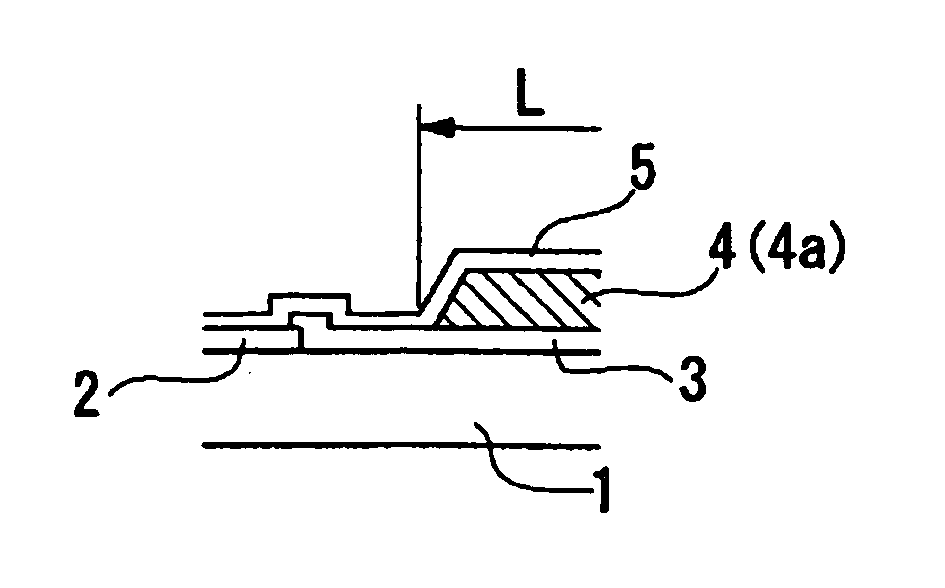
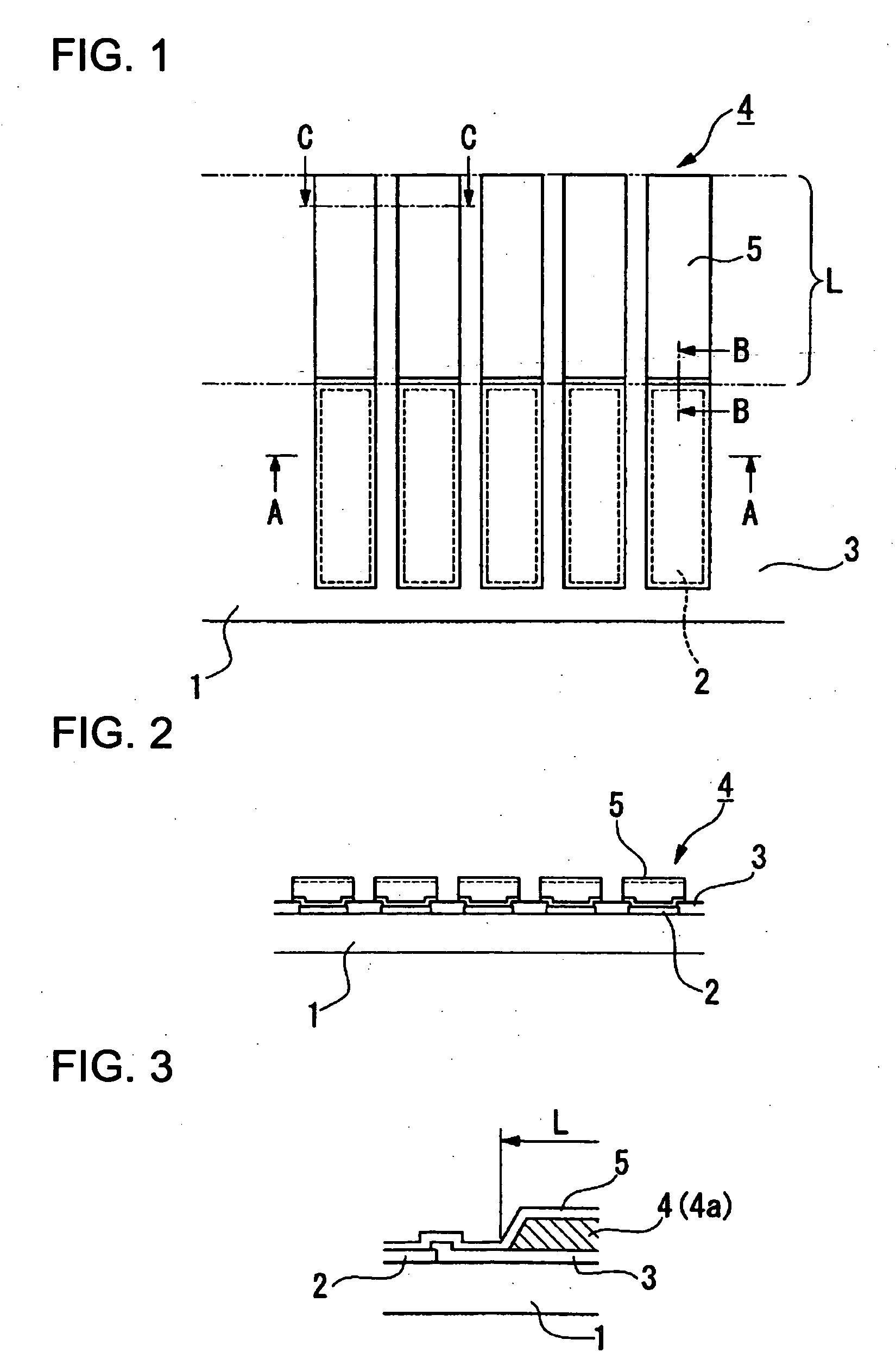
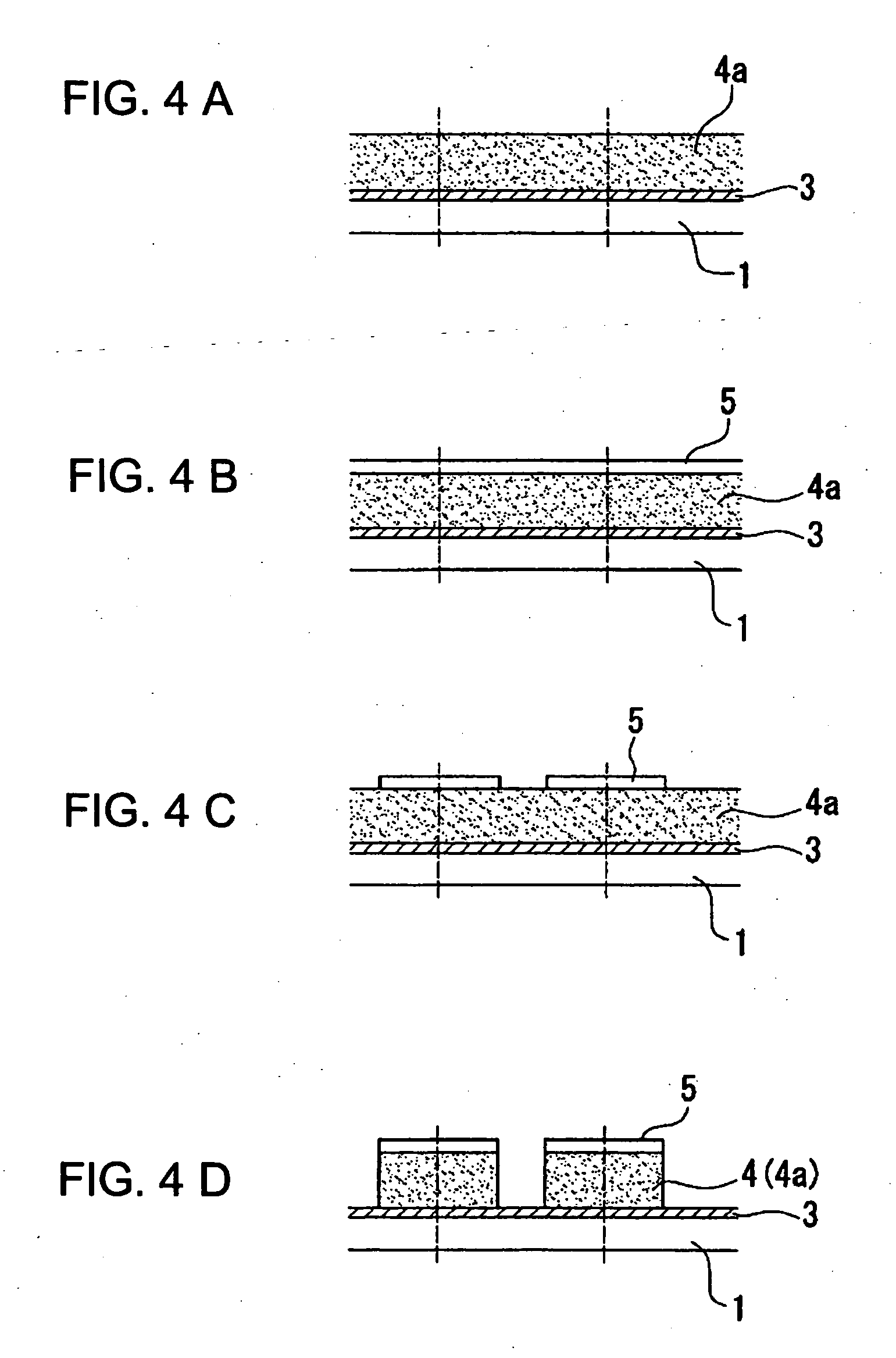
[0030] The embodiments of the semiconductor device, the method for manufacturing the same, the circuit substrate, the electro-optical apparatus, and the electronic equipment according to the present invention will be described below with reference to FIG. 1 to FIG. 10. Here, the structure of the semiconductor device used in the manufacturing method of the present invention and an example of the manufacturing process thereof will be described in advance of descriptions of steps specific to the present invention.

[0031]FIG. 1 is a partial plan view of a semiconductor element serving as a semiconductor device according to the present invention. FIG. 2 is a sectional view of the section indicated by a line A-A shown in FIG. 1. FIG. 3 is a sectional view of the section indicated by a line B-B shown in FIG. 1. The semiconductor element in the present embodiment may be a semiconductor substrate, e.g., a silicon wafer in a condition in which a plurality of semiconductor chips are provided, ...


PUM


Abstract

A semiconductor device is provided with a plurality of protrusions which are made of a resin and which protrude higher than electrodes, and conductive layers which are electrically connected to the electrodes and which cover the top surfaces of the protrusions. A method for manufacturing the semiconductor device includes a step of applying a layer of the resin to the semiconductor device except for the electrodes, a step of patterning the conductive layers on the electrodes and the layer of the resin in accordance with the protrusions, and a step of removing the layer of the resin located between the conductive layers by the use of the patterned conductive layers as masks so as to form the protrusions.

Description

CROSS REFERENCE TO RELATED APPLICATIONS [0001] This application is a divisional application of U.S. Ser. No. 10 / 726,275 filed Dec. 2, 2003 which claims priority to Japanese Application No. 2002-350337 filed Dec. 2, 2002, all of which are incorporated by reference.BACKGROUND OF THE INVENTION [0002] 1. Technical Field of the Invention [0003] The present invention relates to a semiconductor device, a method for manufacturing the same, a circuit substrate, an electro-optical apparatus, and electronic equipment. [0004] 2. Description of the Related Art [0005] Conventionally, so-called Au bumps are frequently used for mounting semiconductor devices, e.g., driver ICs. In the formation of the Au bump, a seed layer made of TiW / Au or the like is sputtered on a semiconductor element, a resist is patterned and, thereafter, Au electroplating is applied up to a height on the order of 20 μm. However, it is predicted that stable formation of bumps, such as formation of a resist having a high aspect...

Claims


Application Information

Patent Timeline
IPC IPC(8): G02F1/13G02F1/1345H01L21/3205H01L21/60H01L23/485H01L23/52
CPCH01L24/11H01L2924/01004H01L2924/01013H01L2924/01022H01L2924/01029H01L2924/0103H01L2924/01033H01L2924/01074H01L2924/01078H01L2924/01079H01L2924/04941H01L2924/19041H01L2924/19043H01L2924/3025H01L2924/01005H01L2924/01006H01L2924/01024H01L21/4846H01L2924/00013H01L2224/1161H01L2224/024H01L2224/0236H01L2224/11622H01L2224/13008H01L2224/13666H01L24/13H01L2224/02375H01L2224/02377H01L2224/05124H01L2224/1145H01L2224/1146H01L2224/11901H01L2224/13013H01L2224/1319H01L2224/13582H01L2224/13644H01L2224/114G02F1/13458H01L2224/0401H01L2224/13099H01L2224/13599H01L2224/05599H01L2224/05099H01L2224/29099H01L2224/29599H01L2924/00014H01L2924/14H01L2924/181H01L2924/00H01L21/60H01L23/485H01L24/02H01L24/14H01L2224/12105H01L2224/13018
Inventor ITO, HARUKI
Owner SEIKO EPSON CORP
Why Eureka
Try Eureka