Semiconductor device, method for manufacturing semiconductor device, and display

a semiconductor device and semiconductor technology, applied in the direction of semiconductor devices, thermoelectric device junction materials, electrical apparatus, etc., can solve the problems of low production efficiency of semiconductor devices, process yield decline, and difficulty in adequately setting both carriers, so as to improve production efficiency and simplify the structure of the display apparatus, the production process of the display apparatus can be simple and the effect of improving production efficiency

Inactive Publication Date: 2010-06-10
IDEMITSU KOSAN CO LTD +1
View PDF21 Cites 44 Cited by
  • Summary
  • Abstract
  • Description
  • Claims
  • Application Information

AI Technical Summary

Benefits of technology

[0048]By this, the display apparatus becomes simple in the structure since it uses the semiconductor device having light-emitting function and transistor function. As a result, the production process of the display apparatus can be simple and production efficiency can be improved.
[0049]According to the invention, carrier balance can be easily stabilized in comparison with the semiconductor device having an organic semiconductor layer made only of an organic substance, since the semiconductor device has the light-emitting part composed of the organic semiconductor layer and the oxide semiconductor layer. As a result, production efficiency can be improved.

Problems solved by technology

However, in such a semiconductor device, it is difficult to adequately set both of the carriers injected and process yield decreases because the light-emitting part is made only of organic substances.
Hence, such a semiconductor device has disadvantage of low production efficiency.

Method used


Image

  • Semiconductor device, method for manufacturing semiconductor device, and display
  • Semiconductor device, method for manufacturing semiconductor device, and display
  • Semiconductor device, method for manufacturing semiconductor device, and display

Examples


first embodiment

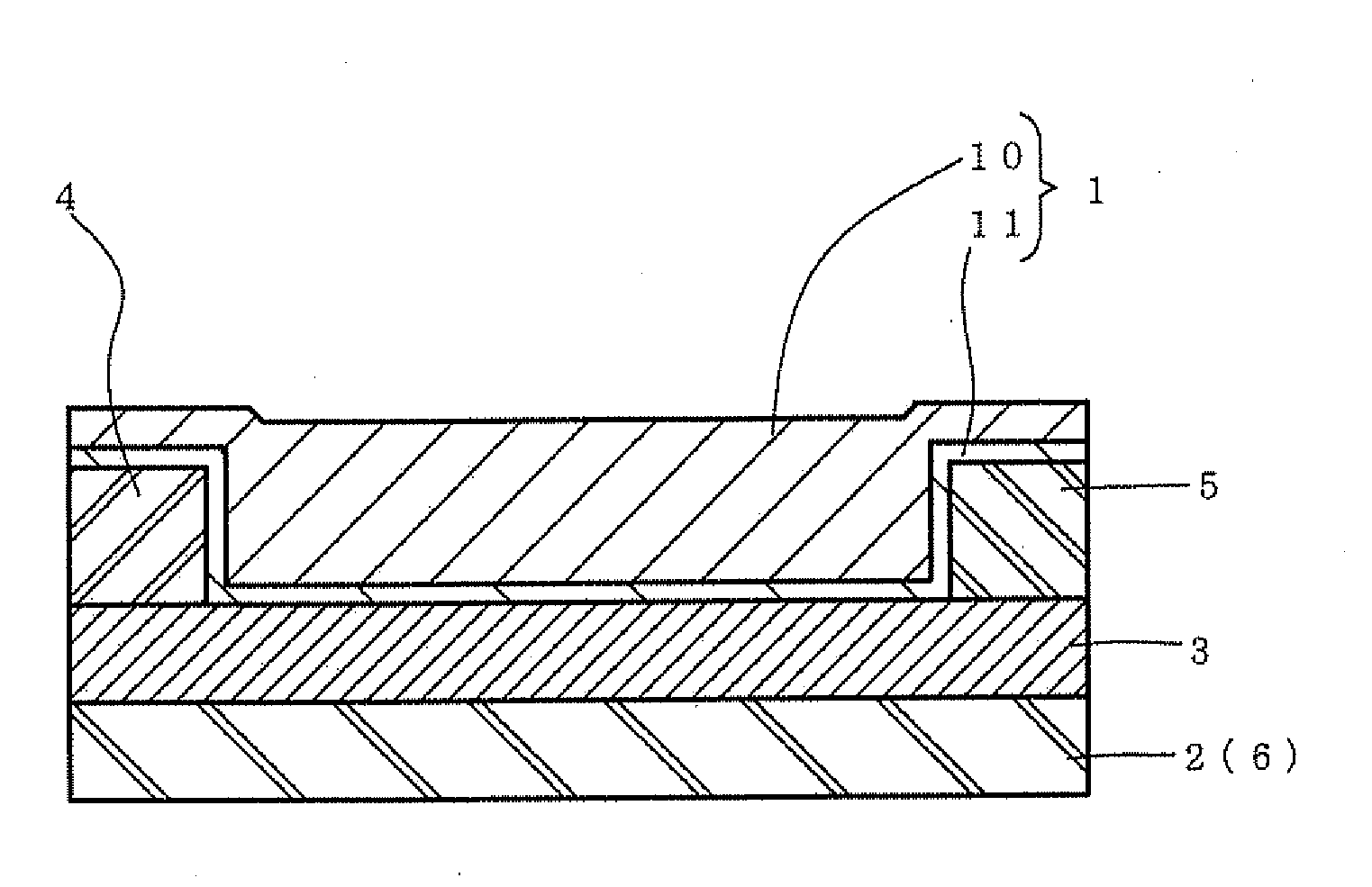
[0071]FIG. 1 is a schematic cross-sectional view of the semiconductor device according to the first embodiment of the invention.

[0072]As shown in FIG. 1A, the semiconductor device comprises an light-emitting part 1 formed from an organic semiconductor layer 10 and an oxide semiconductor layer 11, and emits light due to recombination of holes and electrons within the light-emitting part 1.

[0073]Specifically, light emission may be generated at the organic semiconductor layer 10, the oxide semiconductor layer 11 or both thereof, or the interface of the organic semiconductor layer 10 and the oxide semiconductor layer 11, as long as it is within the light-emitting part 1. Light emission is preferably generated at the organic semiconductor layer 10, or in the vicinity of the interface of the organic semiconductor layer 10 and the oxide semiconductor layer 11.

[0074]The semiconductor device of this embodiment comprises a light-emitting part 1 formed from an organic semiconductor layer 10 an...

second embodiment

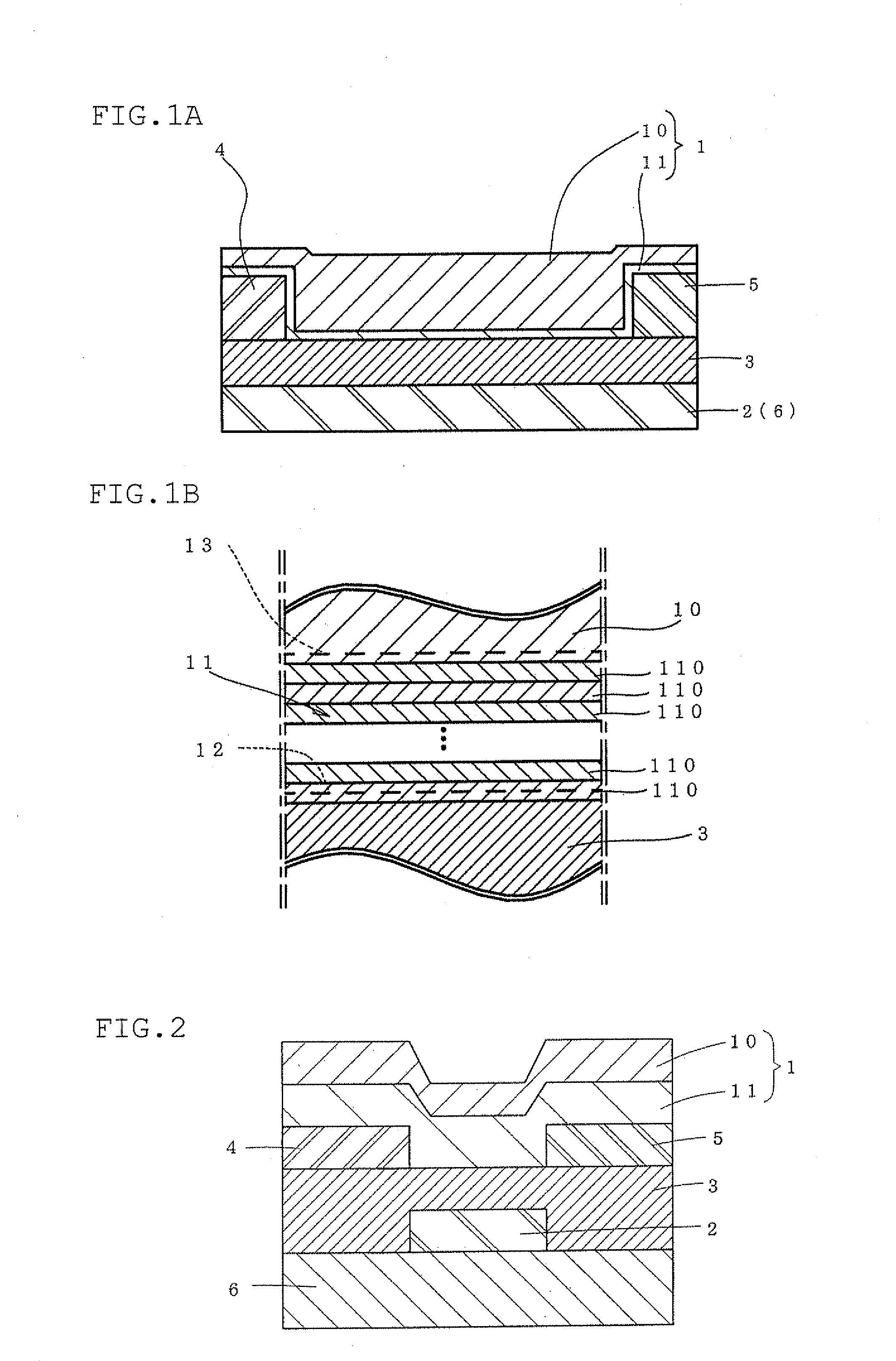
[0167]FIG. 2 is a schematic cross-sectional view of the semiconductor device according to the second embodiment of the invention.

[0168]The semiconductor device of this embodiment is almost the same as the above-mentioned embodiment but is different in the point where the substrate 6 and the first electrode 2 are formed separately.

[0169]Namely, in the semiconductor device of this embodiment, the first electrode 2 distinct from the substrate 6 is provided in the central part of the substrate 6. The first electrode 2 is formed of the material used for the second and third electrodes 4 and 5 in the above-mentioned first embodiment. The insulator layer 3 is provided on the substrate 6 and the first electrode 2.

[0170]The other constitutions are the same as the above-mentioned ones.

[0171]The semiconductor device of this embodiment is used as a tight-emitting element in the same as the above-mentioned embodiment. The operations and effects are almost the same as above.

[0172]According to the...

third embodiment

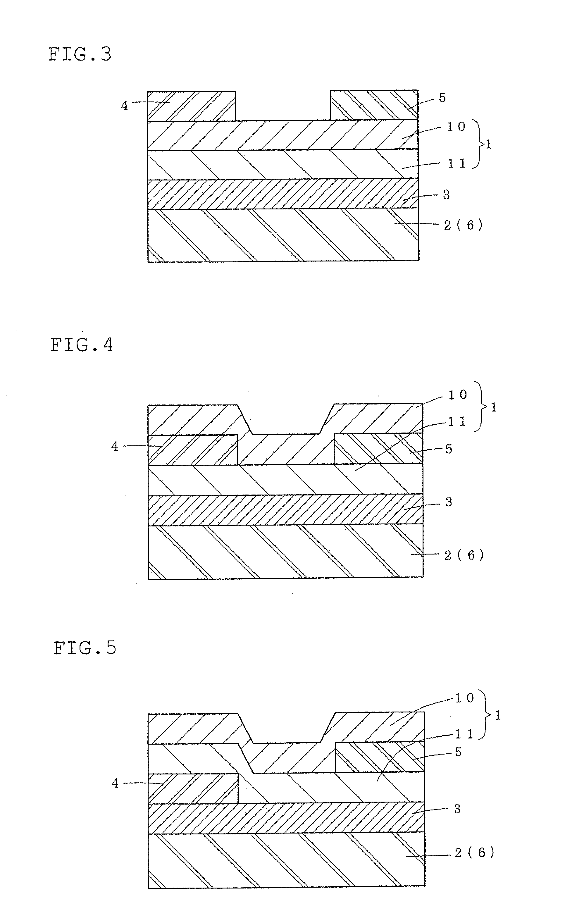
[0173]FIG. 3 is a schematic cross-sectional view of the semiconductor device according to the third embodiment of the invention.

[0174]The semiconductor device of this embodiment has the constitution, in which the second and third electrodes 4 and 5 are disposed on the upper side of the organic semiconductor layer 10 but not between the insulator layer 3 and the oxide semiconductor layer 11, and which is different from the above-mentioned embodiments.

[0175]According to the semiconductor layer having the constitution, mobility of the transistor can be adjusted to be high, since the electric field between the first electrode 2 and the second and third electrodes 4 and 5 is effectively applied to the oxide semiconductor layer 11 and the organic semiconductor layer 10.


PUM


Abstract

A semiconductor device includes an organic semiconductor layer 10 and an oxide semiconductor layer 11, and emits light.

Description

TECHNICAL FIELD[0001]The invention relates to a semiconductor device using an organic substance and emitting light, a method of producing the semiconductor device and a display apparatus using the semiconductor device.BACKGROUND ART[0002]Recently, organic semiconductors using organic substances have gathered attention as materials used for semiconductors.[0003]In general, such organic substances used for the organic semiconductors have advantages such that they can be easily formed into a film by using a simple film-forming method such as spin coating or vacuum deposition, and that the temperature during the production process thereof can be lowered in comparison with the conventional semiconductor devices using amorphous or polycrystalline silicon. Such lowering process temperature allows to form a film on a plastic substrate having lower heat resistance, to decrease the display weight and costs, and to give various applications having the advantage of flexibility of the plastic su...

Claims


Application Information

Patent Timeline
Patent Type & Authority Applications(United States)
IPC IPC(8): H01L51/52H01L51/56
CPCH01L29/7869H01L51/0054H01L51/5203H01L51/0562H01L51/52H01L51/0545H10K85/622H10K10/486H10K10/466H10K50/80H10K50/805H10K50/30
Inventor YANO, KOKINAKANOTANI, HAJIMEADACHI, CHIHAYA
Owner IDEMITSU KOSAN CO LTD
Why Eureka
Try Eureka