

Shift register
a shift register and shift register technology, applied in the field of shift registers, can solve the problems of increasing layout area and power consumption of clock interconnection, and achieve the effects of reducing interconnection between circuits, reducing layout area and power consumption of shift registers, and reducing interconnections between circuits
- Summary
- Abstract
- Description
- Claims
- Application Information
AI Technical Summary
Benefits of technology
Problems solved by technology
Method used
Image

Examples
first embodiment
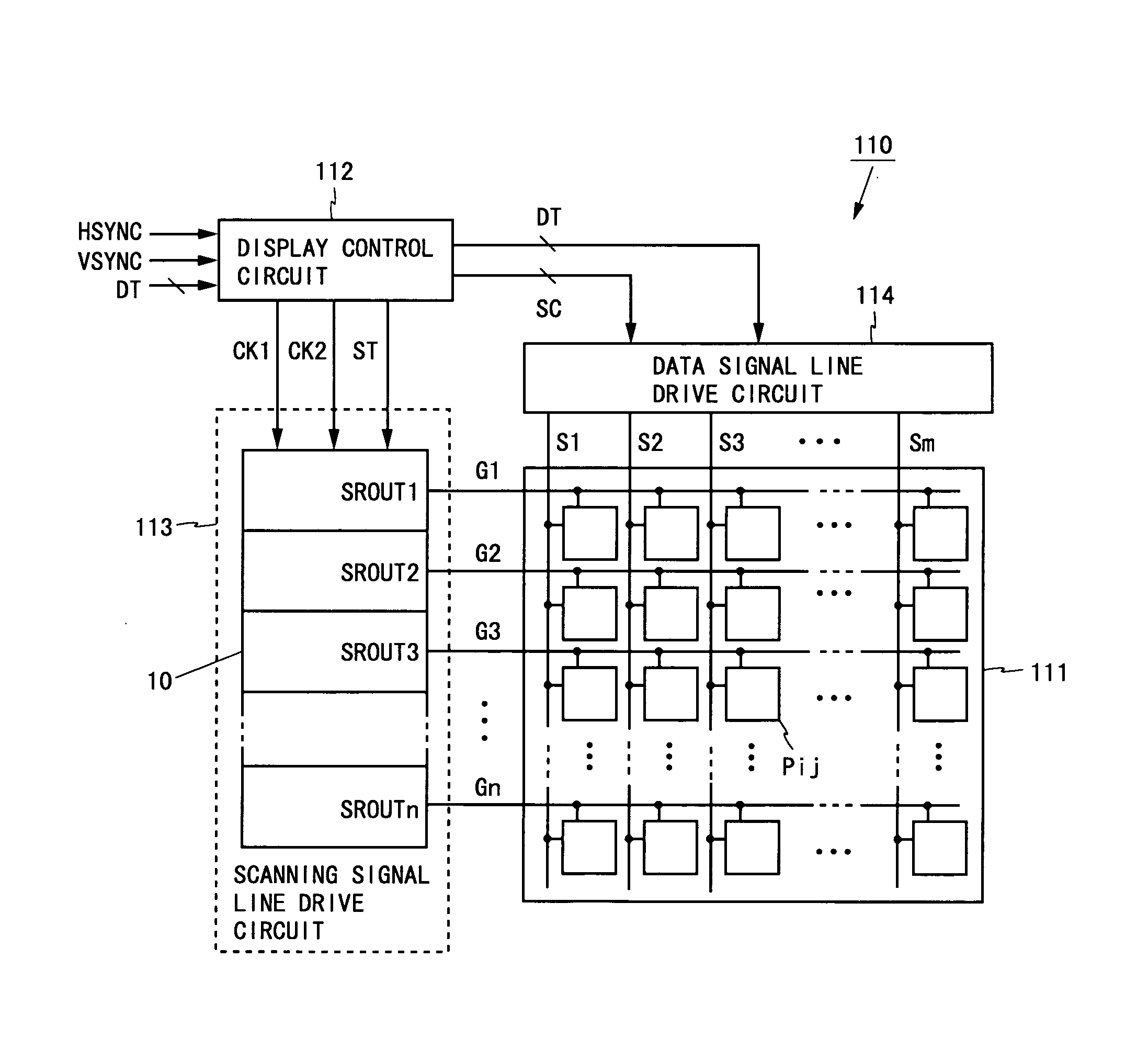
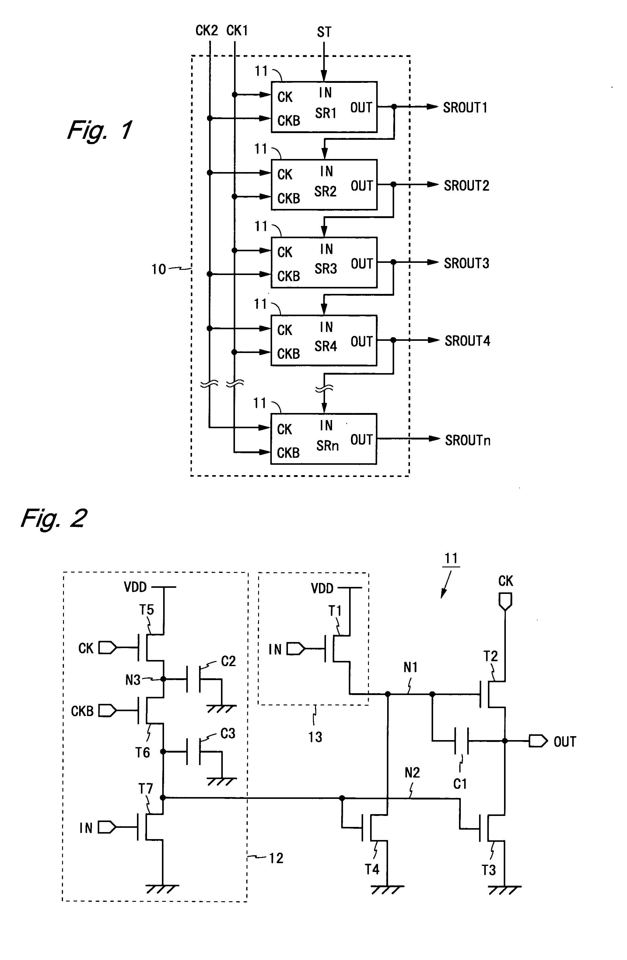
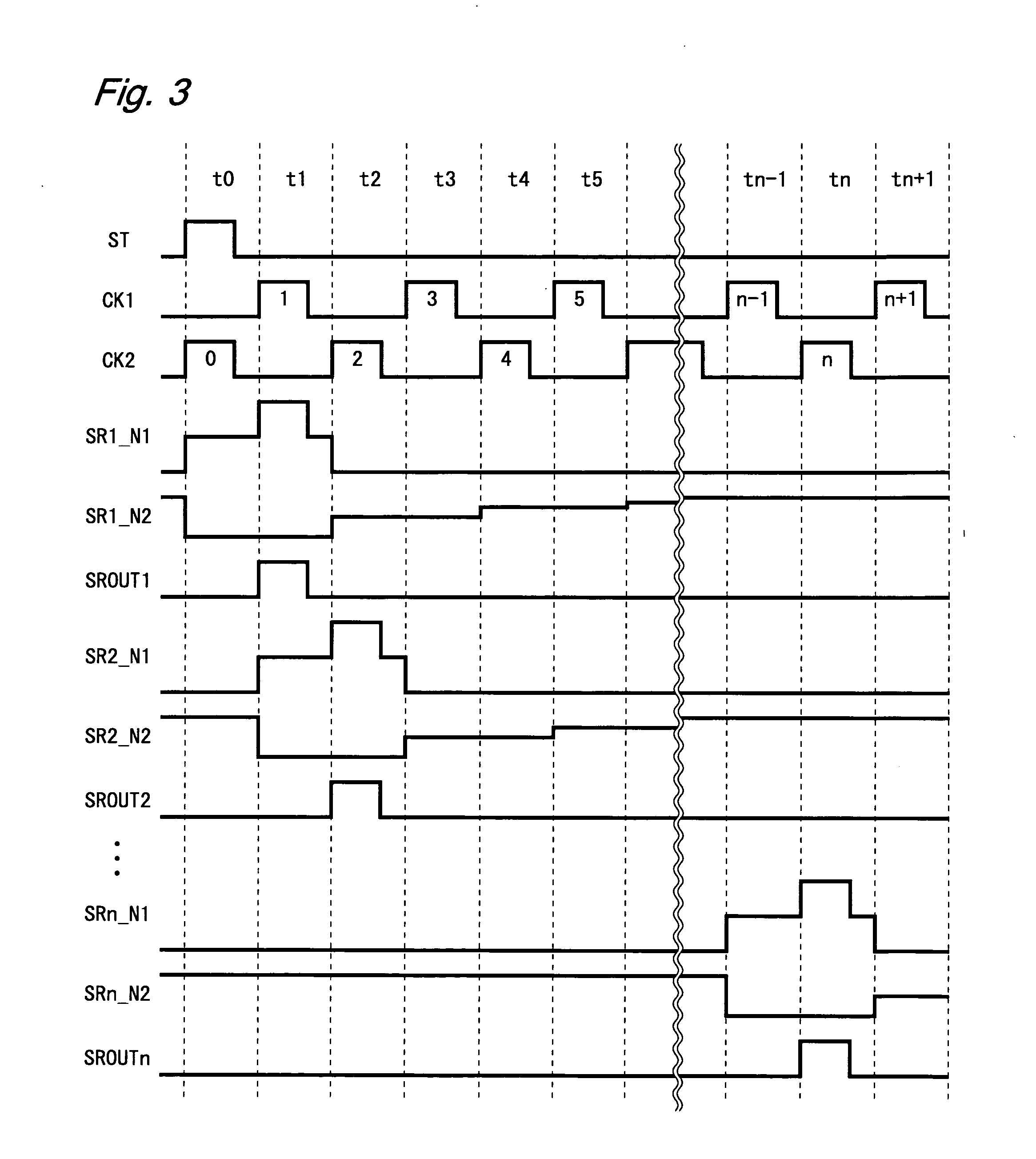
[0080]FIG. 1 is a block diagram showing a configuration of a shift register according to a first embodiment of the present invention. The shift register 10 shown in FIG. 1 has a configuration in that n (n: an integer of two or more) unit circuits 11 are cascaded. The unit circuit 11 has a clock terminal CK, a clock terminal CKB, an input terminal IN and an output terminal OUT. In the following, signals to be input / output via the respective terminals are described using designations equal to the relevant terminals. (For example, a signal to be input via the clock terminal CK is referred to as a clock signal CK.)
[0081]A start pulse ST and two-phase clock signals CK1 and CK2 are supplied externally to the shift register 10. The start pulse ST is supplied to the input terminal IN of the first unit circuit 11. The clock signal CK1 is supplied to the clock terminal CK of the odd-numbered unit circuit 11 and the clock terminal CKB of the even-numbered unit circuit 11. The clock signal CK2 ...
second embodiment
[0115]FIG. 7 is a block diagram showing a configuration of a shift register according to a second embodiment of the present invention. The shift register 20 shown in FIG. 7 includes n unit circuits 21 each having a scanning direction switch terminal UD, a scanning direction switch terminal UDB, an input terminal INu and an input terminal INd. The shift register 20 corresponds to the shift register 10 according to the first embodiment to which a function of switching a scanning direction (a direction of shift of an output signal) is added.
[0116]In the shift register 20, a direction along which a number of the unit circuit 21 becomes large (a downward direction in FIG. 7) is referred to as a forward direction, and a reverse direction thereof (an upward direction in FIG. 7) is referred to as a backward direction. The unit circuit 21 having the number which is smaller by one is referred to as a forward unit circuit, and the unit circuit 21 having the number which is larger by one is ref...
third embodiment
[0123]FIG. 9 is a block diagram showing a configuration of a shift register according to a third embodiment of the present invention. The shift register 30 shown in FIG. 9 includes n unit circuits 31 each having an initialization terminal INIT. The shift register 30 corresponds to the shift register 10 according to the first embodiment to which an initializing function is added. In the unit circuit 31, the initialization terminal INIT is supplied with an initialization signal INIT given externally.
[0124]FIG. 10 is a circuit diagram of the unit circuit 31 included in the shift register 30. The unit circuit 31 shown in FIG. 10 corresponds to the unit circuit 11 according to the first embodiment to which an initialization circuit 32 including an N-channel type transistor T13 is added. The transistor T13 has a drain terminal applied with a power supply voltage VDD, a source terminal connected to a node N2, and a gate terminal connected to the initialization terminal INIT.
[0125]When the ...
PUM
 Abstract
Description
Claims
Application Information