Apparatus and method for combined micro-scale and nano-scale c-v, q-v, and i-v testing of semiconductor materials

a semiconductor material and micro-scale technology, applied in the direction of individual semiconductor device testing, scanning probe techniques, instruments, etc., can solve the problems of adverse effects on the signal to noise ratio of measurement, adverse effects on the properties of the device to be measured, and reduction of the sampled area, so as to reduce the measurement area and small capacitance variations

Inactive Publication Date: 2010-06-17
MULTIPROBE
View PDF6 Cites 31 Cited by
  • Summary
  • Abstract
  • Description
  • Claims
  • Application Information

AI Technical Summary

Benefits of technology

[0012]Further enabling the measurement of very small capacitance variations is the combination of other measurements such as current measurements or charge measurements. Novel sensor designs permitting both CV and IV measuremen

Problems solved by technology

It is undesirable to construct such test structures on wafers thereby effectively sacrificing them.
Furthermore, the deposition process may adversely affect the properties of t

Method used


Image

  • Apparatus and method for combined micro-scale and nano-scale c-v, q-v, and i-v testing of semiconductor materials
  • Apparatus and method for combined micro-scale and nano-scale c-v, q-v, and i-v testing of semiconductor materials
  • Apparatus and method for combined micro-scale and nano-scale c-v, q-v, and i-v testing of semiconductor materials

Examples


Embodiment Construction

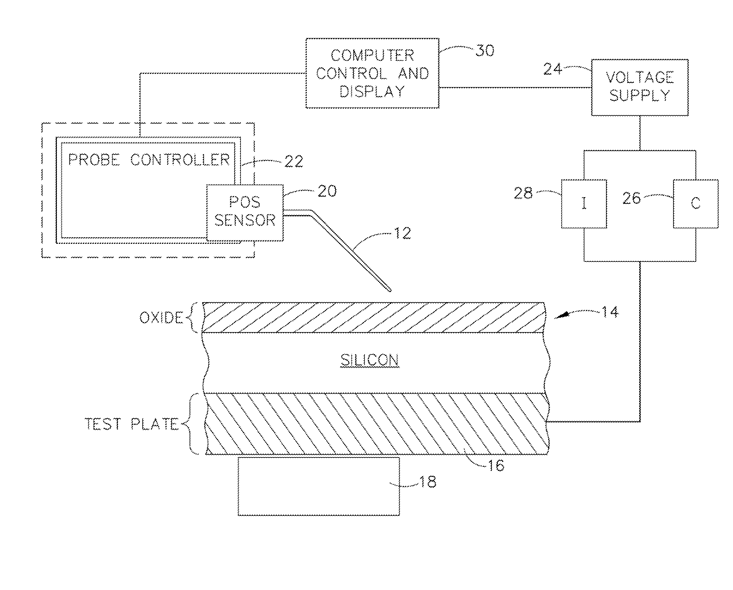
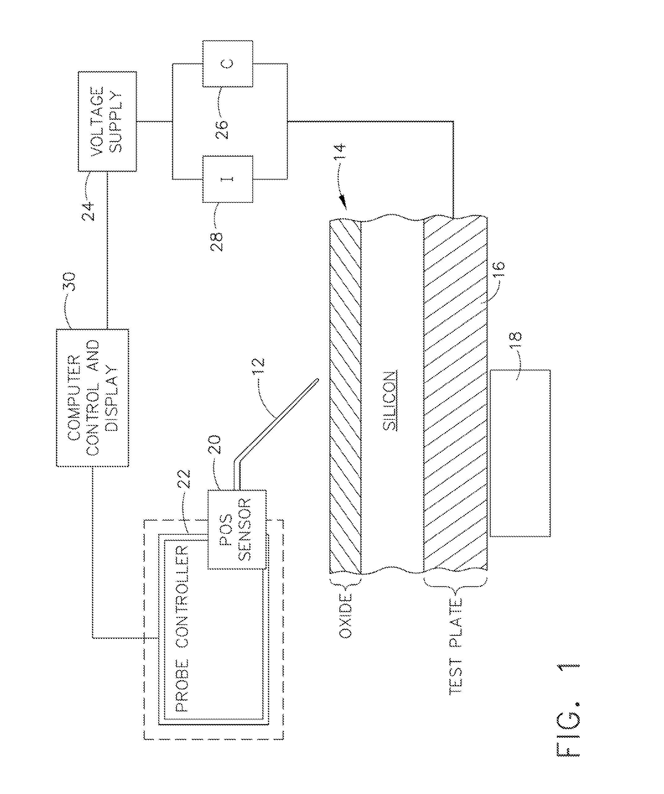
[0040]Referring to the drawings, FIG. 1 shows schematically the elements of a system 10 embodying the invention. A probe 12 is employed for contact with a semiconductor wafer 14 under test. The wafer is supported, by a test plate 16 of a probe station translation stage 18. A position sensor 20 senses the contact by the probe on the semiconductor surface, as will be described in greater detail subsequently. A probe controller 22 such as is disclosed in U.S. Pat. No. 3,345,567 Turner et. al, which is incorporated into this specification by reference can ‘be used to position the probe with respect to the surface of the semiconductor if the structures to be probed are lame enough to be seen optically or if the structure to be probed is uniform such as a semiconductor wafer and precise positioning is not required. If the structure to be probed is too small to be seen with optical microscopes, then a separate means must be employed to locate the feature and position the probe relative to ...


PUM


Abstract

Current Voltage and Capacitance Voltage (IV and CV) measurements are critical in measurement of properties of electronic materials especially semiconductors. A semiconductor testing device to accomplish IV and CV measurement supports a semiconductor wafer and provides a probe for contacting a surface on the wafer under control of an atomic Force Microscope or similar probing device for positioning the probe to a desired measurement point on the wafer surface. Detection of contact by the probe on the surface is accomplished and test voltage is supplied to the semiconductor wafer. A first circuit for measuring capacitance sensed by the probe based on the test voltage and a complimentary circuit for measuring Fowler Nordheim current sensed by the probe based on the test voltage are employed with the probe allowing the calculation of characteristics of the semiconductor wafer based on the measured capacitance and Fowler Nordheim current.

Description

REFERENCE TO RELATED APPLICATIONS[0001]This patent application claims the priority of U.S. Provisional Patent Application Ser. No. 60 / 807,678 filed on Jul. 18, 2006 having the same title as the present application, the disclosure of which is incorporated fully herein by reference.BACKGROUND OF THE INVENTION[0002]1. Field of the Invention[0003]This patent relates generally to the field of electrical characterization of materials and structures and, more particularly, to a non-destructive testing device and method for characterization of semiconductor materials using combined C-V and I-V testing using atomic force probing. It also pertains to the use of multiple probes on a semiconductor device at the nanoscale in order to enable new, novel combinations of measurements of current, charge, and capacitance.[0004]2. Description of the Related Art[0005]It is well known that in the processing and fabrication of semiconductor structures, it is advantageous to measure their performance and p...

Claims


Application Information

Patent Timeline
IPC IPC(8): G01R31/02G01R31/26G01R27/26
CPCG01R31/312G01Q60/30G01Q60/38G01R27/2605G01R31/2601G01R31/2648
Inventor ERICKSON, ANDREW N.
Owner MULTIPROBE
Why Eureka
Try Eureka