Magnetic storage device

Active Publication Date: 2010-06-17
RENESAS ELECTRONICS CORP
View PDF20 Cites 0 Cited by
  • Summary
  • Abstract
  • Description
  • Claims
  • Application Information

AI Technical Summary

Benefits of technology

[0036]According to the invention, the following is implemented even when the respective magnetizations of the first and second ferromagnetic films included in the anchoring layer in antiparallel state is made closer to parallel state by the synthetic magnetic field arising from the first and second wirings: the magnetic moment of the entire anchoring layer is prevented from becoming so large that

Problems solved by technology

However, conventional MRAMs involve the following problems:
In high-integration devices, such as MRAMs, it is virtually impossible to make the recording layers identical in shape in all magnetic storage elements and thi

Method used


Image

  • Magnetic storage device
  • Magnetic storage device
  • Magnetic storage device

Examples


Example

First Embodiment

Circuitry and Structure of Memory Cells

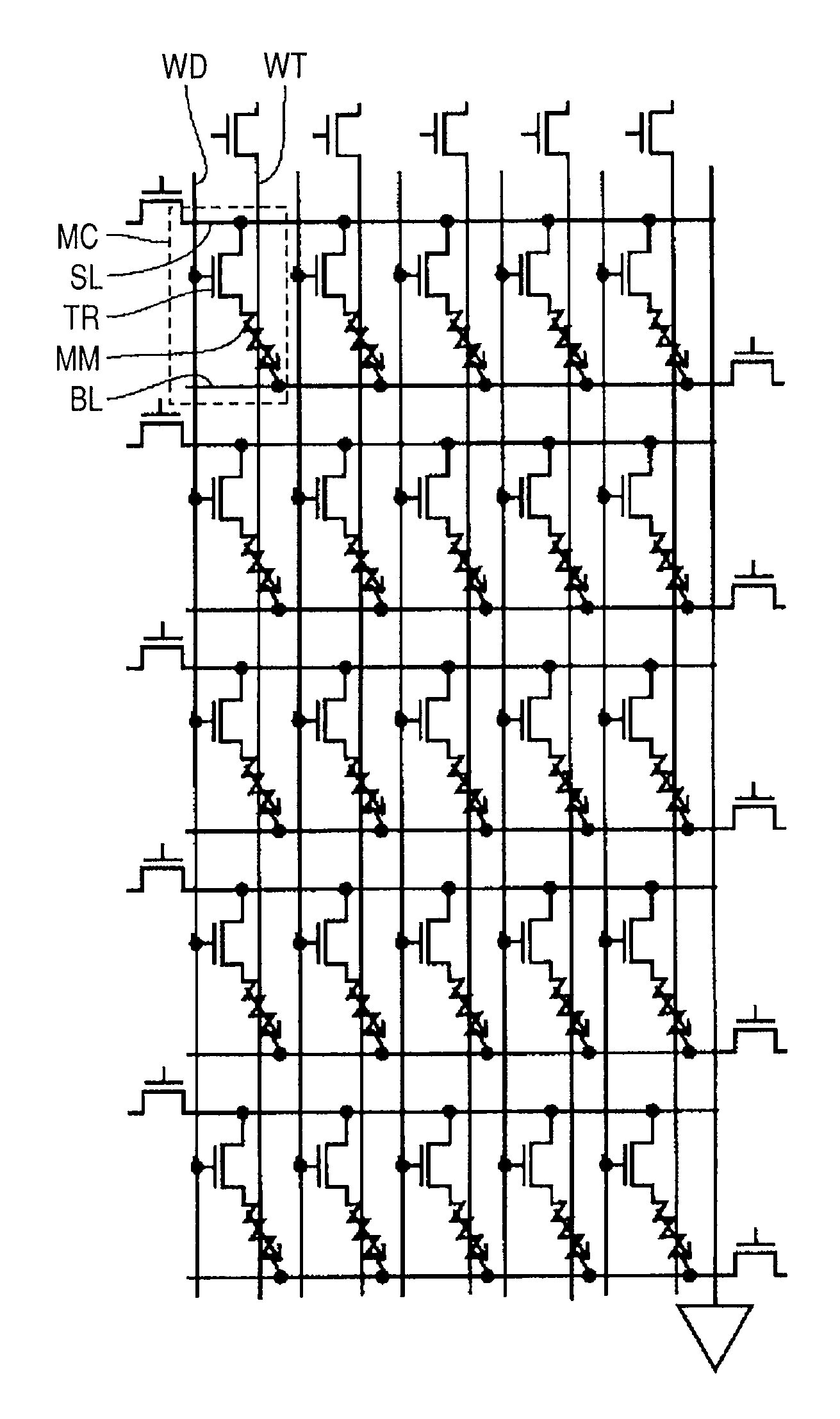
[0062]First, description will be given to the circuitry of memory cells of a magnetic storage device in the first embodiment of the invention. FIG. 1 is a circuit diagram of memory cells of the magnetic storage device in the first embodiment of the invention.

[0063]In the magnetic storage device, as illustrated in FIG. 1, one memory cell MC (in dotted frame) is comprised of an element selection transistor TR and a magnetic storage element (ferromagnetic tunnel junction element) MM. Multiple memory cells MC are formed in a matrix pattern.

[0064]A write line WT and a bit line BL for rewriting and reading information cross this magnetic storage element MM. A bit line BL is electrically coupled to one end of each of magnetic storage elements MM arranged in juxtaposition in one direction (for example, in rows).

[0065]The write lines WT are so arranged that a magnetic field can be applied to each of magnetic storage elements MM arranged ...

Example

Second Embodiment

[0155]FIG. 21 is a plan view schematically illustrating the planar shape of a recording layer of a magnetic storage device in a second embodiment of the invention. The cross section structure in this embodiment is the same as in the first embodiment.

[0156]The curved portions 704a and 704b are different from each other in curvature and this recording layer is asymmetric in the direction of hard axis of magnetization. In this recording layer, the substantial easy axis of shape is inclined from the first straight line 63. With respect to the asteroid curve in this case, the magnitude of current as well as the direction of current differs when “1” or “0” is written, as described in relation to plot 36 in FIG. 12. Also in this case, however, the influence of the magnetization of the anchoring layer can be suppressed by providing the recording layer with the laminated structure illustrated in FIG. 4.

[0157]Any difference in the magnitude of current at the time of writing “...

Example

Third Embodiment

[0160]FIG. 22 is a sectional view schematically illustrating the laminated structure of a recording layer of a magnetic storage device in a third embodiment of the invention. The planar shape of this recoding layer is the same as in the first embodiment.

[0161]Description will be given to this embodiment mainly with reference to FIG. 22. The magnetic storage device in this embodiment has a magnetic storage element MMv in place of the magnetic storage element MM (FIG. 4). The magnetic storage element MMv has a recording layer 3v in place of the recording layer 3 in the magnetic storage element MM (FIG. 4).

[0162]The recording layer 3v has such a structure that a ferromagnetic film 3a, a nonmagnetic film 3c (third nonmagnetic film), a ferromagnetic film 3d (fourth ferromagnetic film), and a nonmagnetic metal film 3b are laminated in this order over the tunnel insulating layer 2. The ferromagnetic film 3a is comprised of a cobalt alloy film and is 2 nm in thickness and th...


PUM


Abstract

A magnetic storage device stable in write characteristic is provided. A first nonmagnetic film is provided over a recording layer. A first ferromagnetic film is provided over the first nonmagnetic film and has a first magnetization and a first film thickness. A second nonmagnetic film is provided over the first ferromagnetic film. A second ferromagnetic film is provided over the second nonmagnetic film, is coupled in antiparallel with the first ferromagnetic film, and has a second magnetization and a second film thickness. An antiferromagnetic film is provided over the second ferromagnetic film. The sum of the product of the first magnetization and the first film thickness and the product of the second magnetization and the second film thickness is smaller than the product of the magnetization of the recording layer and the film thickness of the recording layer.

Description

CROSS-REFERENCE TO RELATED APPLICATIONS[0001]The disclosure of Japanese Patent Application No. 2008-318617 filed on Dec. 15, 2008 including the specification, drawings and abstract is incorporated herein by reference in its entirety.BACKGROUND OF THE INVENTION[0002]The present invention relates to magnetic storage devices and in particular to a magnetic storage device having a recording layer and an anchoring layer.[0003]Magnetoresistive (MR) effect is a phenomenon that when a magnetic field is applied to a magnetic material, its electrical resistance varies and this phenomenon is utilized in magnetic field sensors, magnetic heads, and the like. As giant magnetoresistance (GMR) effect materials that exert especially profound magnetoresistance effect, artificial lattice films of Fe / Cr, Co / Cu, and the like are introduced in Non-patent Documents 1 and 2.[0004]There is proposed a magnetoresistance effect element using a laminated structure of a ferromagnetic layer (free layer) / nonmagnet...

Claims


Application Information

Patent Timeline
IPC IPC(8): G11B5/706
CPCG11C11/16Y10T428/1143G11B5/66G11C11/161G11C11/1659
Inventor TAKENAGA, TAKASHIKUROIWA, TAKEHARUTAKADA, HIROSHIMATSUDA, RYOJITAKEUCHI, YOSUKE
Owner RENESAS ELECTRONICS CORP
Why Eureka
Try Eureka