Methods for concealing surface defects

a technology of surface defects and defects, applied in the field of surface defects removal, can solve the problems of affecting the production efficiency of the product, and affecting the production efficiency of the product, and achieves the effect of reducing production costs, reducing production costs, and reducing production costs

Inactive Publication Date: 2010-06-24
INTEL CORP
View PDF9 Cites 3 Cited by
  • Summary
  • Abstract
  • Description
  • Claims
  • Application Information

AI Technical Summary

Problems solved by technology

Surface defects that are clearly distinguishable may impair a performance perception of the product, thereby leading to a possible loss of sales.
Surface defects may be introduced at various stages of the semiconductor manufacturing and assembly process.
These, and other various processes, increase the propensity of surfac

Method used


Image

  • Methods for concealing surface defects
  • Methods for concealing surface defects
  • Methods for concealing surface defects

Examples


Embodiment Construction

[0013]In the following description, numerous specific details are set forth in order to provide a thorough understanding of various illustrative embodiments of the invention. It will be understood, however, to one skilled in the art, that embodiments of the invention may be practiced without some or all of these specific details. In other instances, well known process operations have not been described in detail in order not to unnecessarily obscure pertinent aspects of embodiments being described. In the drawings, like reference numerals refer to same or similar functionalities or features throughout the several views.

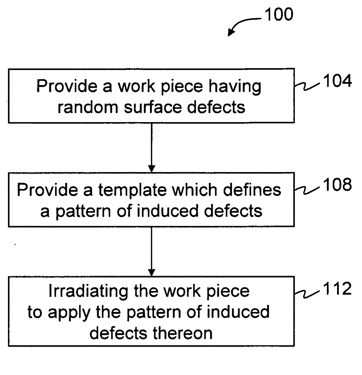
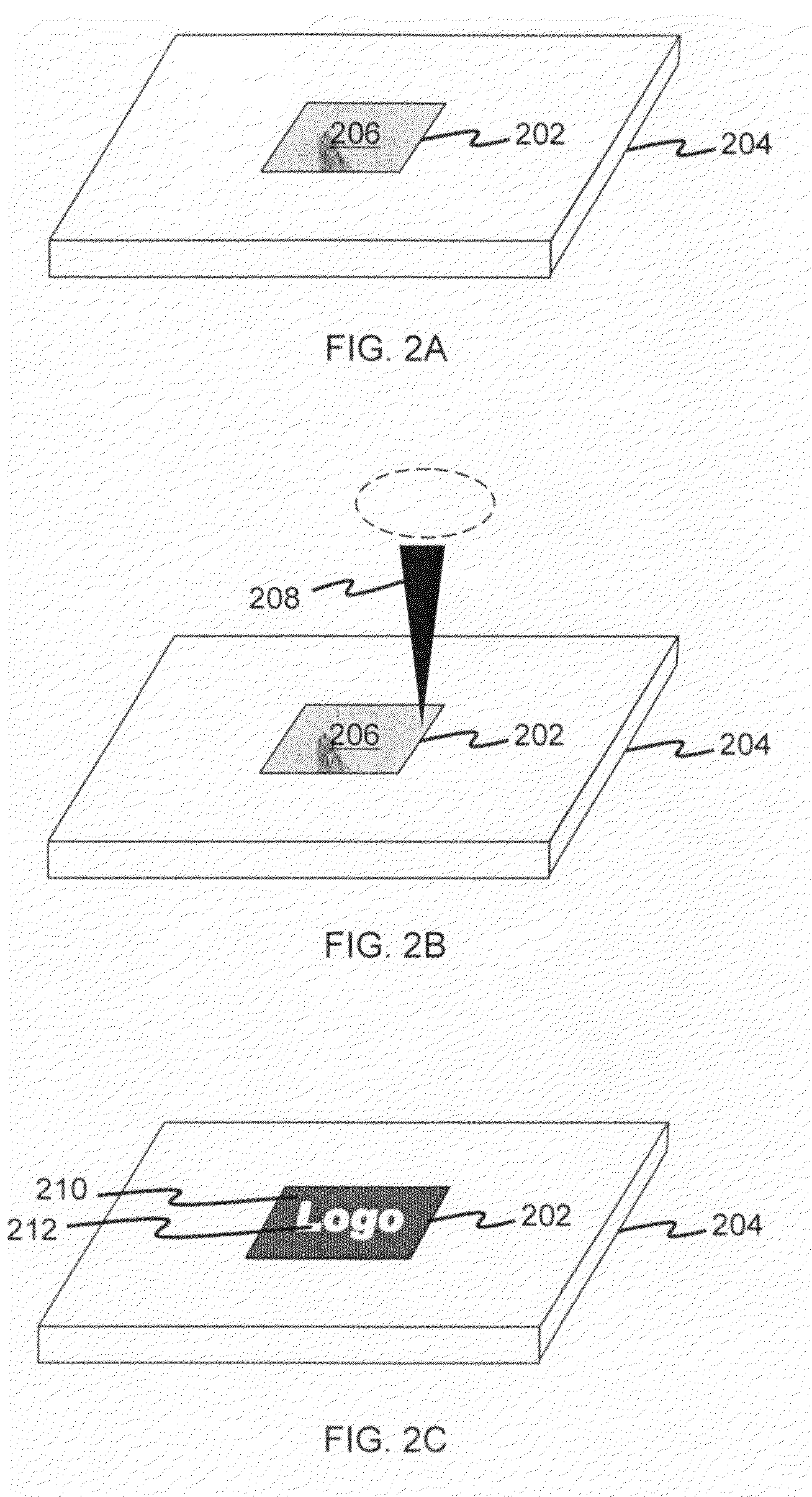
[0014]FIG. 1 is a flow sequence 100 for a method of removing surface defects according to one embodiment of the invention. The flow sequence 100 will be described with further reference to FIGS. 2A to 2C illustrating various process outputs obtained during the flow sequence 100 of FIG. 1.

[0015]The flow sequence 100 begins with providing a work piece having random unco...


PUM


Abstract

Methods for removing random or uncontrolled surface defects from a work piece surface are provided, by applying a plurality of induced controlled defects over the random defects to alter the surface texture.

Description

BACKGROUND [0001]1. Technical Field[0002]Embodiments of the invention relate generally to the field of semiconductor technology and, more particularly, to removal of surface defects using laser ablation methods.[0003]2. Description of Related Art[0004]A key requirement for microelectronics products, such as processor dice, intended for the consumer sector is the visual appearance of the products to be marketed. Very often, consumers place equal importance on the performance as well as the appearance of the products. Surface defects that are clearly distinguishable may impair a performance perception of the product, thereby leading to a possible loss of sales.[0005]Surface defects may be introduced at various stages of the semiconductor manufacturing and assembly process. For example, etch pits may appear on the backside surface of a silicon wafer after micro-fabrication processes such as etching. Scratch marks may be introduced to die back side and edge at the sorting stage. Scuff m...

Claims


Application Information

Patent Timeline
IPC IPC(8): G21K5/10
CPCB23K26/0042B23K26/0066Y10T428/24355Y10T428/2978B23K26/0081B23K26/0006B23K26/352B23K26/354B23K2103/56Y10T428/8305
Inventor VORONOV, SERGEI
Owner INTEL CORP
Why Eureka
Try Eureka