Display apparatus and electronic apparatus

a technology of electronic equipment and display apparatus, which is applied in the field of display equipment and electronic equipment, can solve problems such as the difficulty of compensating for a current variation in a correction process or a similar process, and achieve the effect of suppressing the unevenness of illumination

Inactive Publication Date: 2010-06-24
SONY CORP
View PDF3 Cites 27 Cited by
  • Summary
  • Abstract
  • Description
  • Claims
  • Application Information

AI Technical Summary

Benefits of technology

[0022]With the display apparatus, since a characteristic shift of the transistor which is caused by incidence of light having high energy to the channel of the transistor can be suppressed, decrease of current to flow to an electro-optical element and occurrence of a fault in picture quality such as stripes and luminance unevenness can be suppressed.

Problems solved by technology

Where the R and G subpixels are influenced not only by light emitted from them themselves but also by light emitted from the adjacent subpixel, it is very difficult to compensate for a current variation in a correction process or a like process.

Method used


Image

  • Display apparatus and electronic apparatus
  • Display apparatus and electronic apparatus
  • Display apparatus and electronic apparatus

Examples


embodiment

1. Embodiment

System Configuration

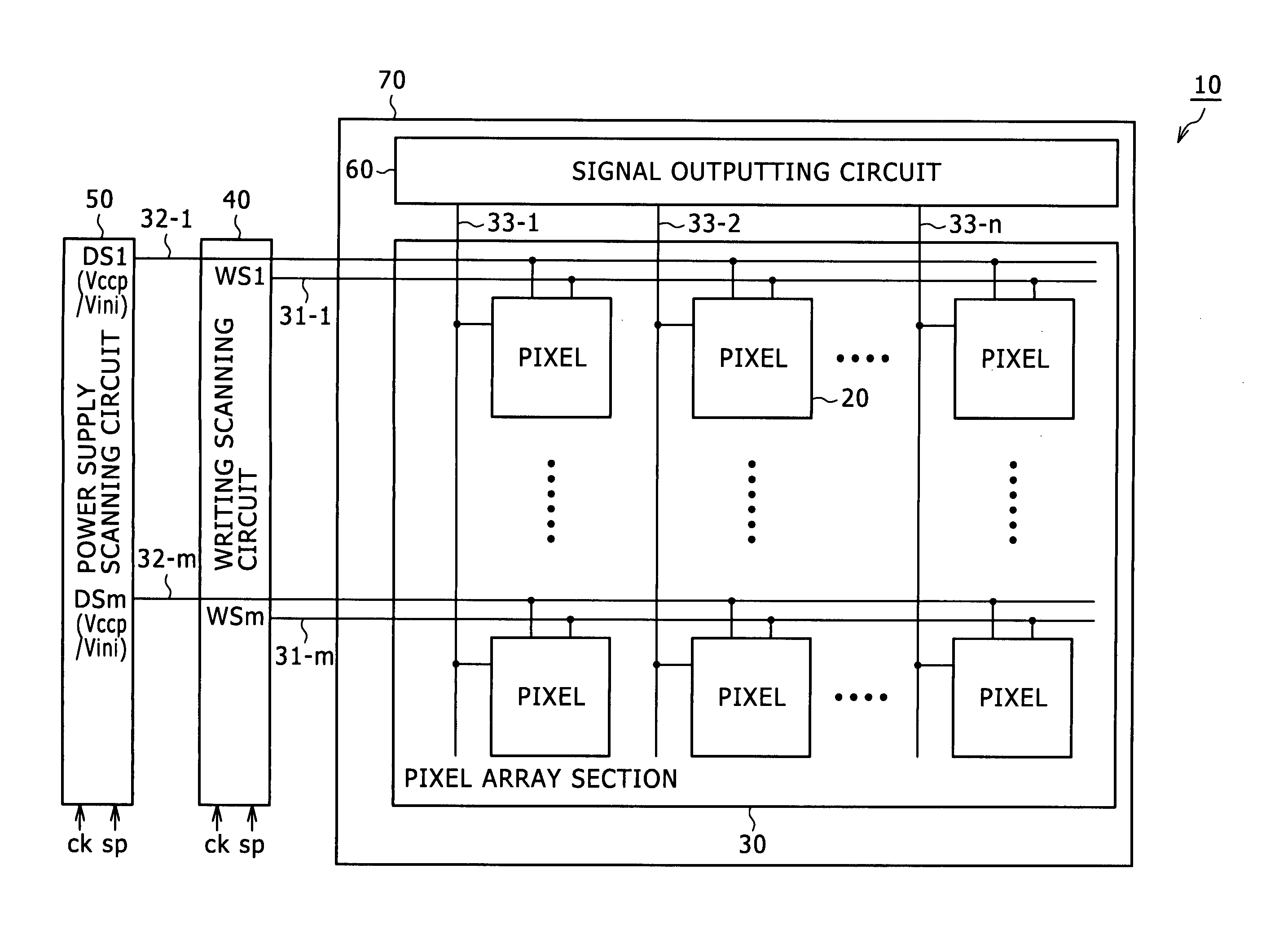
[0049]FIG. 1 is a block diagram showing a general system configuration of an active matrix display apparatus to which an embodiment of the present invention is applied. Here, it is assumed that the active matrix display apparatus described is an active matrix organic EL display apparatus wherein an organic EL element which is an electro-optical element of the current driven type whose emitted light luminance varies in response the value of current flowing through the element is used as a light emitting element of a pixel or pixel circuit.

[0050]Referring to FIG. 1, the organic EL display apparatus 10 shown includes a plurality of pixels 20 each including a light emitting element, a pixel array section 30 in which the pixels 20 are arranged two-dimensionally in rows and columns, that is, in a matrix, and driving sections disposed around the pixel array section 30. The driving sections drive the pixels 20 of the pixel array section 30 to emit light.

[005...

working example 1

1-1. Working Example 1

[0156]FIG. 14 is a plan view showing the light blocking layout structure according to a working example 1. Here, as an example, the light blocking layout structure exhibits a color array wherein R, G and B pixels or subpixels 20R, 20G and 20B are arranged such that the B pixel 20B is positioned centrally and the R and G pixels 20R and 20B are positioned on the opposite sides of the B pixel 20B. FIG. 15 shows a sectional structure of the light blocking layout structure taken along line A-A′ of FIG. 14.

[0157]Since the B pixel 20B is disposed centrally as seen in FIG. 14, transistors in the R and G pixels 20R and 20G positioned on the opposite sides of the B pixel 20B are influenced by irradiation of blue light emitted from the B pixel 20B. In order to prevent incidence of blue light from the B pixel 20B, a metal wiring layer 301G is provided in the layer same as that of the anode electrode of the G pixel 20G on the writing transistor 23, on the organic EL element...

modification 1

to the Working Example 1

[0161]FIG. 16 is a plan view showing a light blocking layout structure according to a modification 1 to the working example 1. In the light blocking layout structure according to the modification 1, light blocking members 303B-1 and 303B-2 having a width greater than the channel width of the writing transistor 23 are provided between R and G pixels 20R and 20B positioned adjacent to and on the opposite sides of the B pixel 20B.

[0162]With the light blocking layout structure according to the modification 1, blue light emitted from the B pixel 20B can be prevented from being reflected by the light blocking members 303G and 303R of the adjacent pixels and entering the B pixel 20B. Accordingly, not only with regard to the R and G pixels 20R and 20B but also with regard to the B pixel 20B, the characteristic shift by an influence of irradiation of blue light can be suppressed to a small amount.


PUM


Abstract

Disclosed herein is a display apparatus, including: a plurality of subpixels disposed adjacent each other and forming one pixel which forms a unit for formation of a color image; the plurality of subpixels including a first subpixel which emits light of the shortest wavelength and a second subpixel disposed adjacent the first subpixel; the second subpixel having a light blocking member disposed between the second subpixel and the first subpixel and having a width greater than a channel length or a channel width of a transistor which forms the second subpixel.

Description

BACKGROUND OF THE INVENTION[0001]1. Field of the Invention[0002]This invention relates to a display apparatus and an electronic apparatus, and more particularly to a display apparatus of the flat type or flat panel type wherein a plurality of pixels each including an electro-optical element are arranged two-dimensionally in rows and columns, that is, in a matrix, and an electronic apparatus which incorporates the display apparatus.[0003]2. Description of the Related Art[0004]In recent years, in the field of display apparatus which display an image, a flat type display apparatus wherein a plurality of pixels or pixel circuits each including a light emitting element are arranged in rows and columns, has been popularized rapidly. One of such flat type display apparatus uses, as a light emitting element of a pixel, an electro-optical element of the current driven type whose emitted light luminance varies in response to the value of current flowing through the element. As the electro-opt...

Claims


Application Information

Patent Timeline
Patent Type & Authority Applications(United States)
IPC IPC(8): G09G5/00G09G3/30
CPCG09G2300/0842G09G2300/0426H01L27/3213G09G3/30G09G2300/0866G09G2320/0233G09G2300/0819H01L27/3253G09G3/3233G09G2300/0452G09G2300/0439G09G3/3275H01L51/5012G09G2320/046H10K59/351H10K59/126H10K50/11H10K59/1275H10K59/123H10K59/131H10K59/35H10K50/86H10K59/1213H10K50/818H10K59/1216G09G3/3225G09G2310/08G09G3/3258G09G3/3266G09G2310/06H01L27/1222H01L27/124H01L27/1255
Inventor YAMAMOTO, TETSUROUCHINO, KATSUHIDE
Owner SONY CORP
Why Eureka
Try Eureka