Phase change memory device

Active Publication Date: 2010-07-01
MICRON TECH INC
View PDF16 Cites 63 Cited by
  • Summary
  • Abstract
  • Description
  • Claims
  • Application Information

AI Technical Summary

Benefits of technology

[0033]During reading, the memory cells are compared with their reference cell(s); thereby it is ensured that any drift affecting an electrical quantity (threshold voltage

Problems solved by technology

The threshold voltage drift is harmful for OTS-selected memory arrays, because it could prevent the storage element of chalcogenic material from being correctly read.
In general, it may be impossible to determine the value of a stored bit if the threshold of the selector switch is not known.
However, currently all the materials suitable for the use in phase change memory devices are affected by the threshold drift.
Furthermore, it has be

Method used


Image

  • Phase change memory device
  • Phase change memory device
  • Phase change memory device

Examples


Embodiment Construction

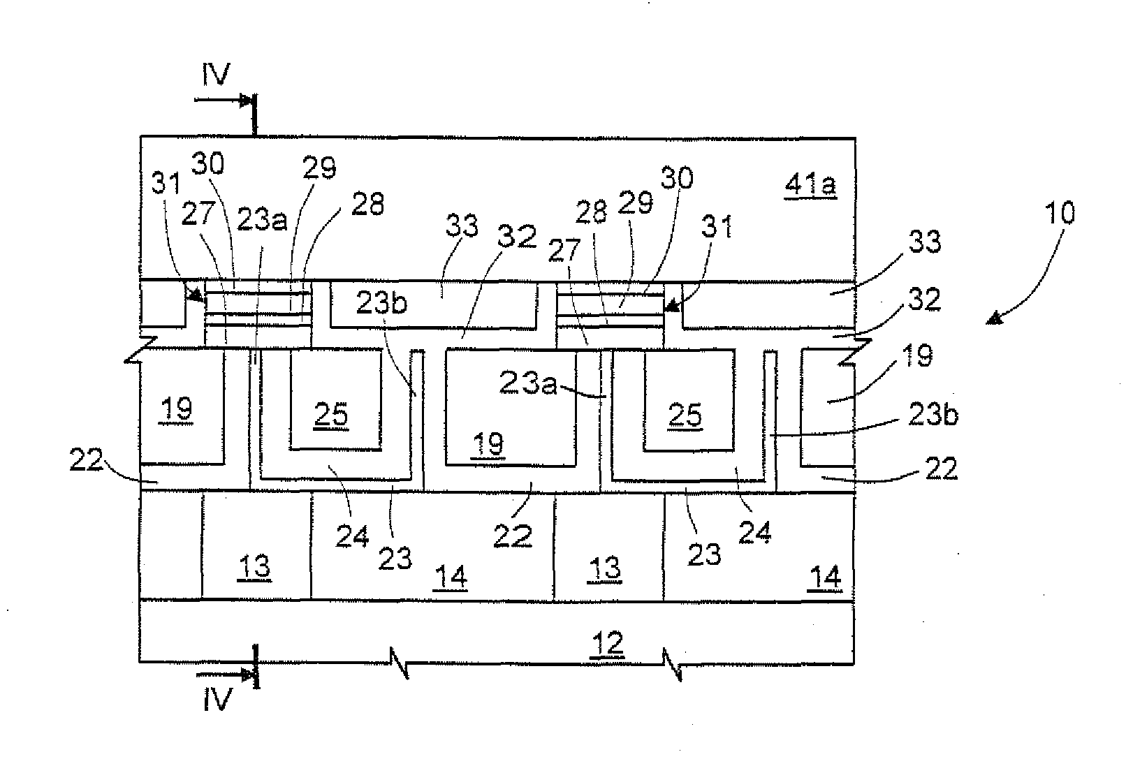
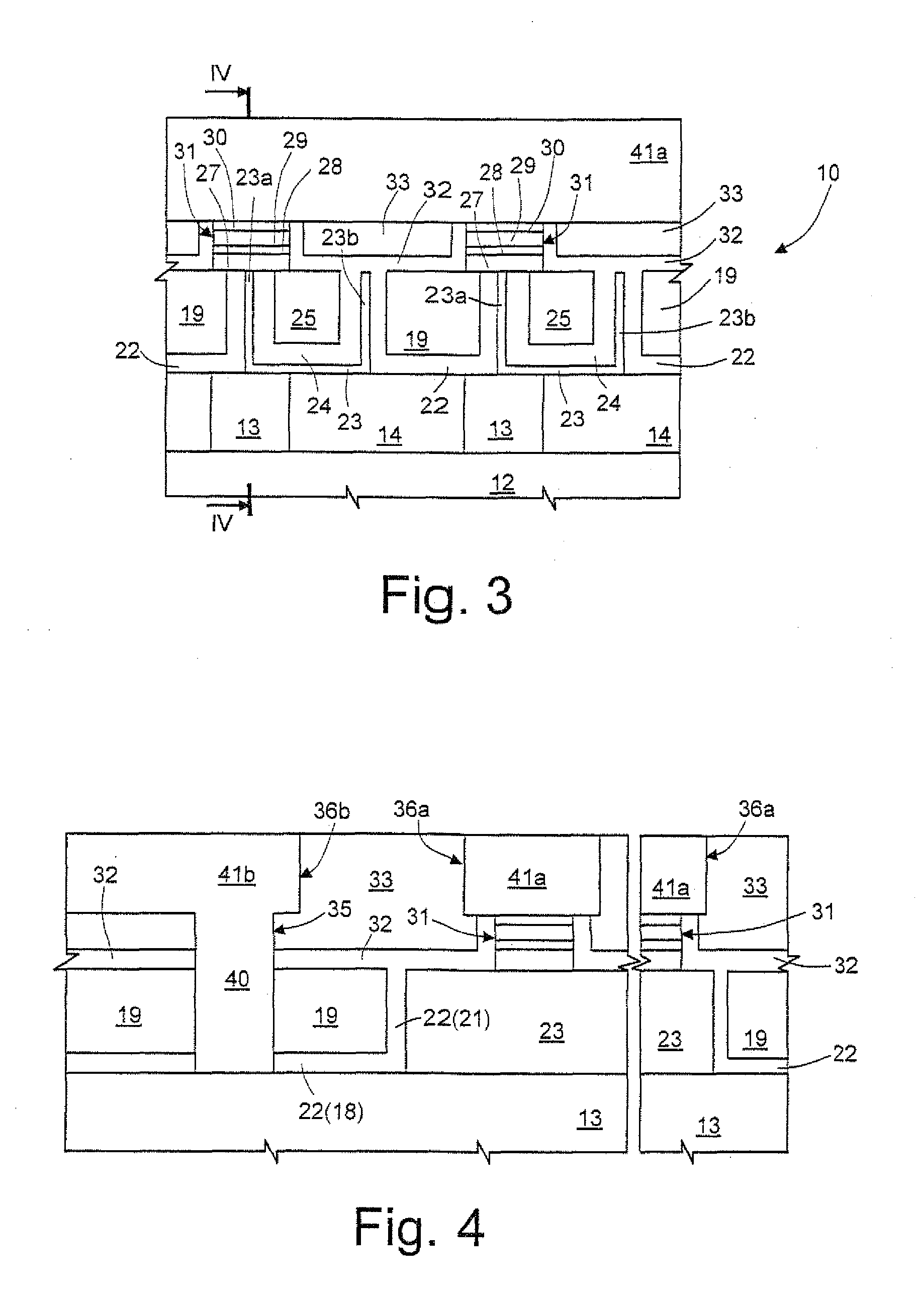
[0047]FIGS. 3 and 4 show an exemplary structure of a phase change memory cell including an ovonic switch.

[0048]In detail, a semiconductor substrate (not shown) is coated with an insulating layer 12. Row lines 13, e.g. of copper, extend on top of the insulating layer 12, insulated from each other by a first dielectric layer 14. A protective region 22 and a first oxide layer 19 encapsulate a heater structure 23 of, e.g., TiSiN, which has a cup-like shape and is internally covered by a sheath layer 24, e.g. of silicon nitride, and filled by a second oxide layer 25.

[0049]The memory cells include PCM / OTS (Ovonic Memory Switch / Ovonic Threshold Switch) stacks or dots 31, each comprising a storage region 27 (e.g., Ge2Sb2Te5), a first barrier region 28 (e.g., TiAlN), a switching region 29 (e.g., As2Se3) and a second barrier region 30 (e.g., TiAlN) extend on and in contact with walls 23a of the heater structures 23. FIG. 3 shows two dots 31 which extend substantially aligned along a column 5 ...


PUM


Abstract

A phase change memory device with memory cells (2) formed by a phase change memory element (3) and a selection switch (4). A reference cell (2a) formed by an own phase change memory element (3) and an own selection switch (4) is associated to a group (7) of memory cells to be read. An electrical quantity of the group of memory cells is compared with an analogous electrical quantity of the reference cell, thereby compensating any drift in the properties of the memory cells.

Description

TECHNICAL FIELD[0001]The present invention relates to a phase change memory device, in particular to a phase change memory device having ovonic threshold switch selectors.BACKGROUND ART[0002]As known, phase change memories use a class of materials that have the property of switching between two phases having distinct electrical characteristics, associated to two different crystallographic structures of the material, and precisely an amorphous, disorderly phase and a crystalline or polycrystalline, orderly phase. The two phases are hence associated to resistivities of considerably different values.[0003]Currently, the alloys of elements of group VI of the periodic table, such as Te or Se, referred to as chalcogenides or chalcogenic materials, can be used advantageously in phase change memory cells. The currently most promising chalcogenide is formed from an alloy of Ge, Sb and Te (Ge2Sb2Te5), which is now widely used for storing information on overwritable disks and has been also pro...

Claims


Application Information

Patent Timeline
IPC IPC(8): G11C11/00G11C7/02G11C5/14
CPCG11C11/56G11C13/0069G11C13/0004G11C13/004G11C2013/0054G11C2213/79H01L27/2427H01L27/2463H01L45/04H01L45/06H01L45/1233H01L45/126H01L45/143H01L45/144G11C11/5678H10B63/24H10B63/80H10N70/231H10N70/20H10N70/826H10N70/8413H10N70/8825H10N70/8828G11C13/02
Inventor PELLIZZER, FABIO
Owner MICRON TECH INC
Why Eureka
Try Eureka