Semiconductor memory device and method of reducing consumption of standby current therein

Active Publication Date: 2010-07-08
SAMSUNG ELECTRONICS CO LTD
View PDF7 Cites 1 Cited by
  • Summary
  • Abstract
  • Description
  • Claims
  • Application Information

AI Technical Summary

Benefits of technology

[0015]It is therefore another feature of an embodiment to provide a method of reducing a standby current in a semiconductor memory device that comprises a memory array including a plurality of bit lines and a plurality of dummy bit lines, comprising: supplying bias voltages having a plurality of voltage levels to the plurality of dummy bit lines; measuring a value of at least one of standby currents between at least one of the plurality of bit lines and at least one of the plurality of dummy bit lines, each of the standby currents being generated by each of the bias voltages; and supplying a bias voltage having any one of the plurality of voltage levels to each of the plurality of dummy bit lines, based on a measured value of a standby current generated by the bias voltage having any one of the plurality of voltage levels.
[0016]It is therefore another feature of an embodiment to provide a method of reducing a standby current in a semiconductor memory device that comprises a memor

Problems solved by technology

A bit line or a word line formed in the edge portion of the memory array may not be able to maintain reliability during a semiconductor manufacturing process.
When a normal cell is replaced with a redundant cell because of its defect, an unwanted standby

Method used


Image

  • Semiconductor memory device and method of reducing consumption of standby current therein
  • Semiconductor memory device and method of reducing consumption of standby current therein
  • Semiconductor memory device and method of reducing consumption of standby current therein

Examples


Embodiment Construction

[0024]Korean Patent Application No. 10-2009-0000384, filed on Jan. 5, 2009, in the Korean Intellectual Property Office, and entitled: “Semiconductor Memory Device,” is incorporated by reference herein in its entirety.

[0025]Exemplary embodiments will now be described more fully hereinafter with reference to the accompanying drawings; however, they may be embodied in different forms and should not be construed as limited to the embodiments set forth herein. Rather, these embodiments are provided so that this disclosure will be thorough and complete, and will fully convey the scope of the invention to those skilled in the art. Like reference numerals refer to like elements throughout.

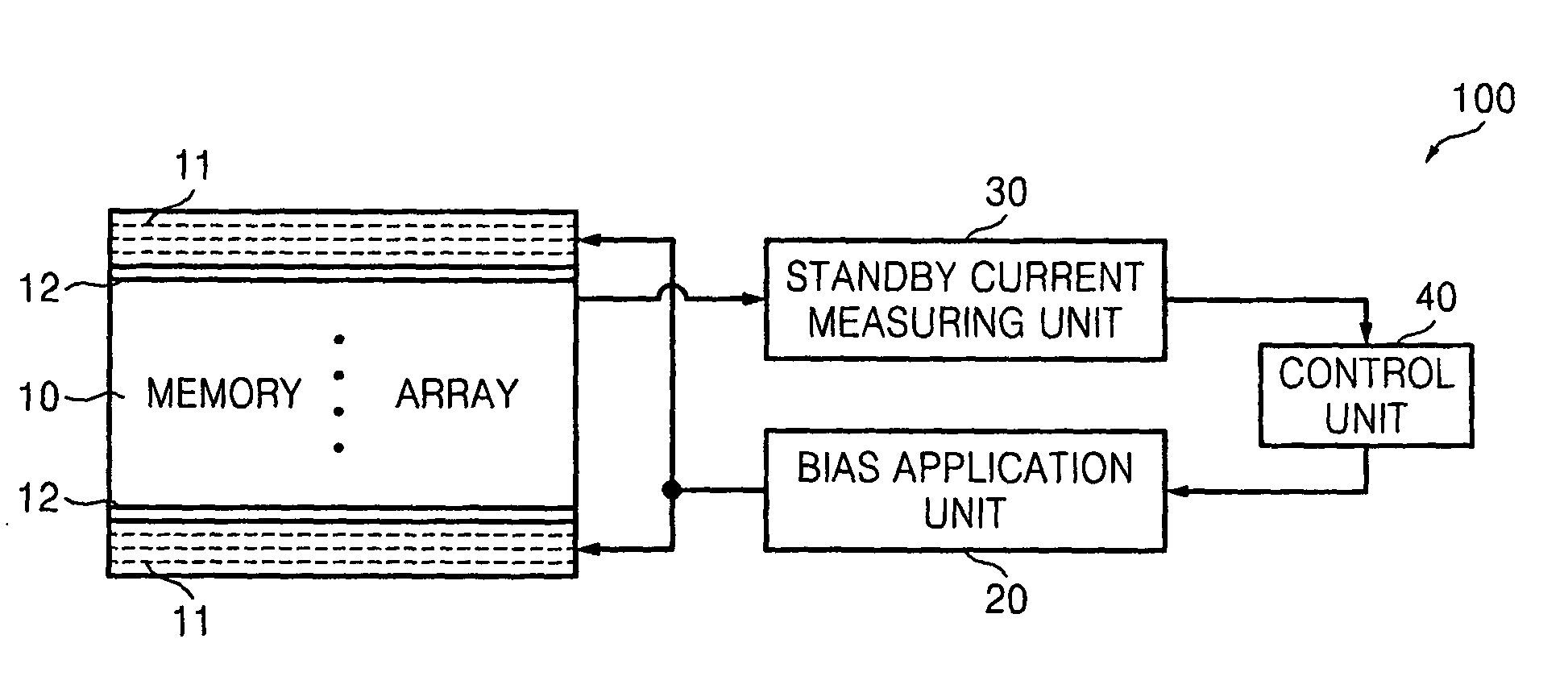
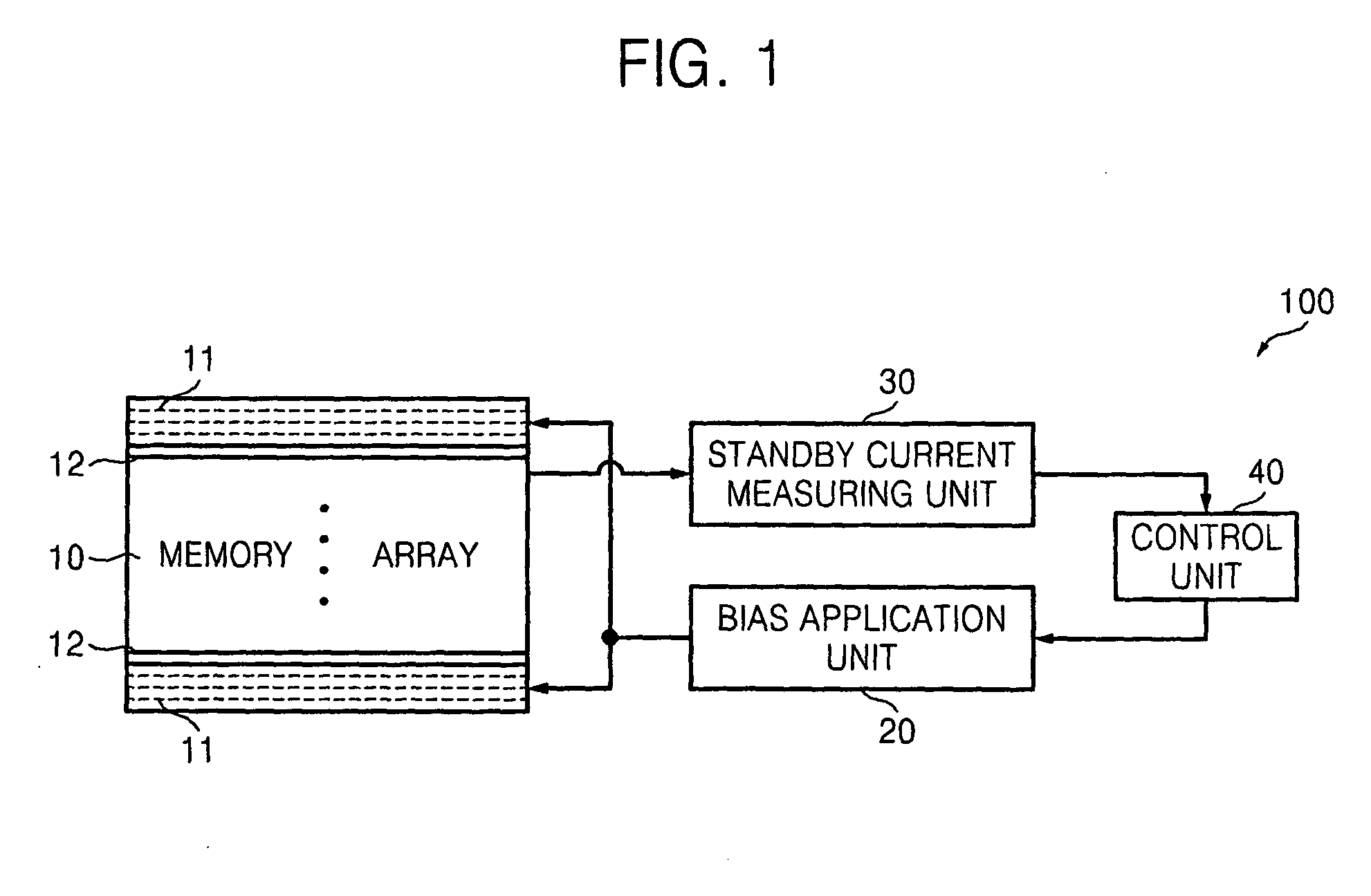
[0026]FIG. 1 is a schematic block diagram of a semiconductor memory device 100 according to an exemplary embodiment. Referring to FIG. 1, the semiconductor memory device 100 may include a memory array 10, a bias application unit 20, and a standby current measuring unit 30.

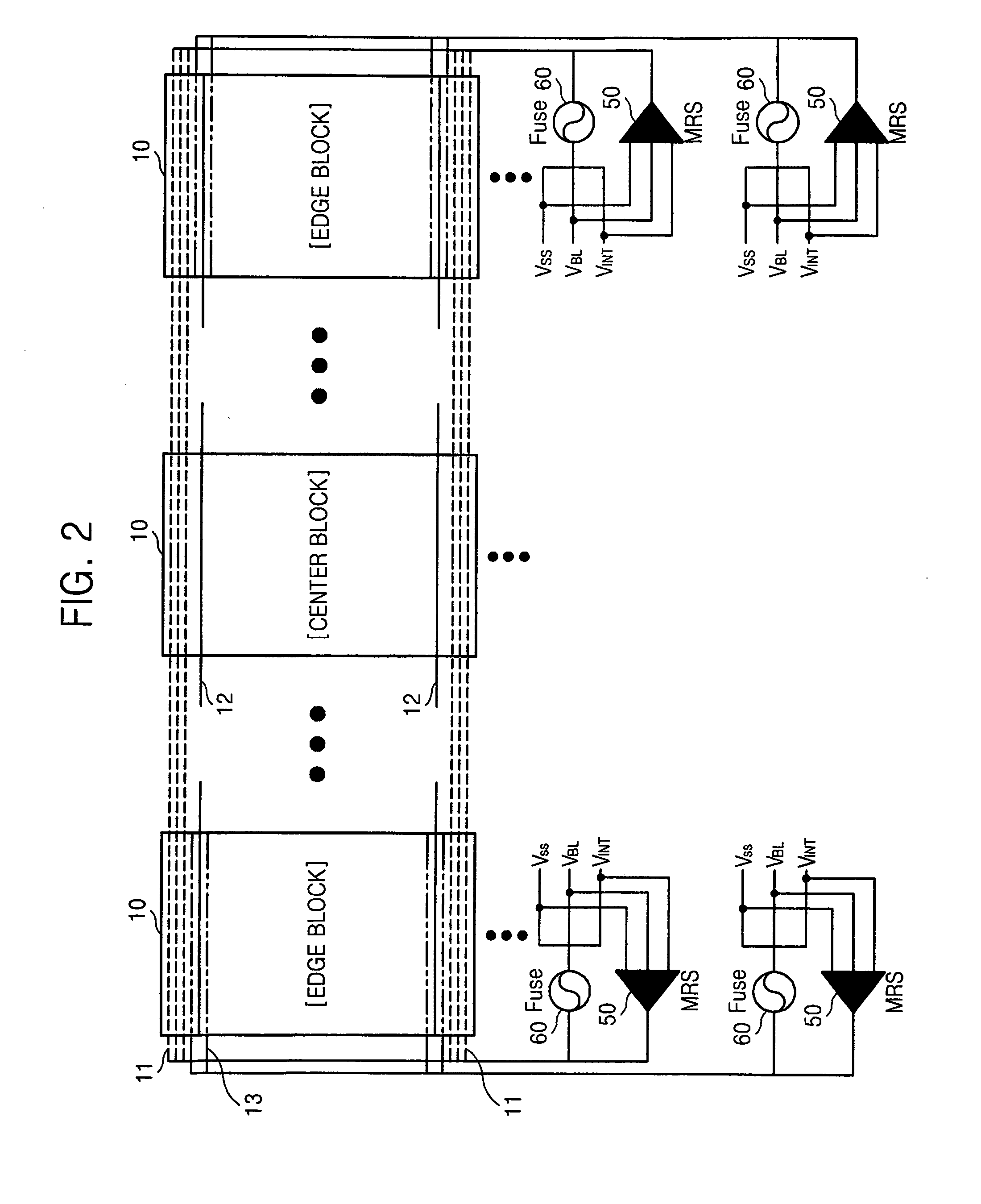
[0027]The memory array 10 may incl...


PUM


Abstract

A semiconductor memory device comprises a memory array including a plurality of bit lines and a plurality of dummy bit lines, a bias application unit configured to supply bias voltages having a plurality of voltage levels to the plurality of dummy bit lines, a standby current measuring unit configured to measure a value of at least one of standby currents between at least one of the plurality of bit lines and at least one of the plurality of dummy bit lines. Each of the standby currents is generated by each of the bias voltages applied by the bias application unit.

Description

BACKGROUND[0001]1. Field[0002]Embodiments relate to a semiconductor device and a controlling method thereof, and more particularly, to a semiconductor memory device in which consumption of a standby current due to an electric current path of a normal cell may be reduced by applying a voltage capable of reducing the standby current to a dummy bit line included in a memory array, and a method of reducing consumption of a standby current therein.[0003]2. Description of the Related Art[0004]In a semiconductor memory device, a memory array may include a dummy cell and a dummy bit line and a dummy word line connected to the dummy cell. A bit line or a word line formed in the edge portion of the memory array may not be able to maintain reliability during a semiconductor manufacturing process. Therefore, the bit or word line in the edge portion may be designated as the dummy bit line or the dummy word line. The dummy bit line or the dummy word line may be excluded from a normal operation of...

Claims


Application Information

Patent Timeline
IPC IPC(8): G11C5/14G11C8/00
CPCG11C5/14G11C7/1045G11C8/12G11C7/22G11C7/14G11C7/12G11C29/50
Inventor LEE, MYUNG-JAEKANG, SANG SEOKLIM, JONG HYOUNG
Owner SAMSUNG ELECTRONICS CO LTD
Why Eureka
Try Eureka