Memory array and method for manufacturing and operating the same
- Summary
- Abstract
- Description
- Claims
- Application Information
AI Technical Summary
Benefits of technology
Problems solved by technology
Method used
Image


Examples
Embodiment Construction
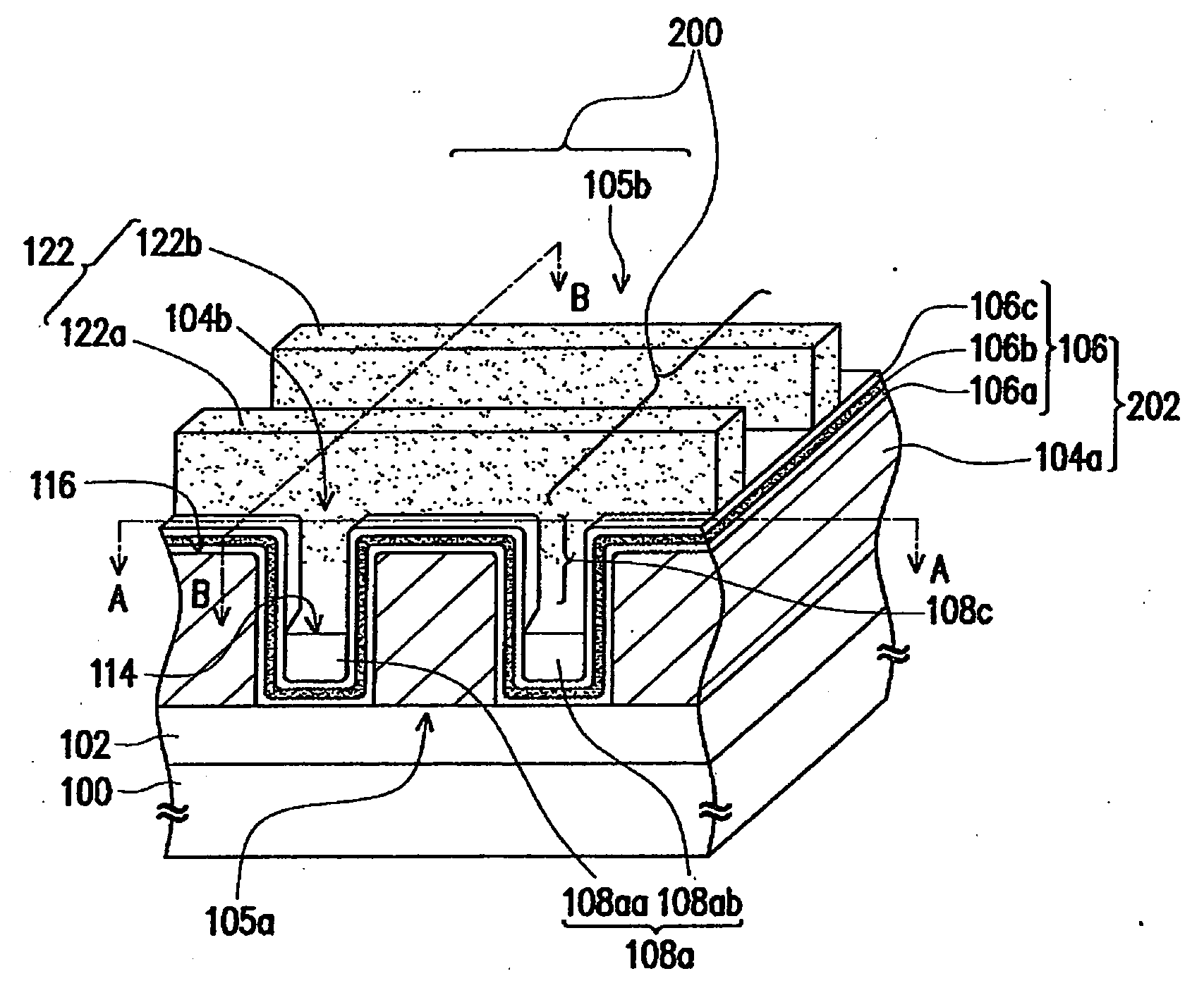
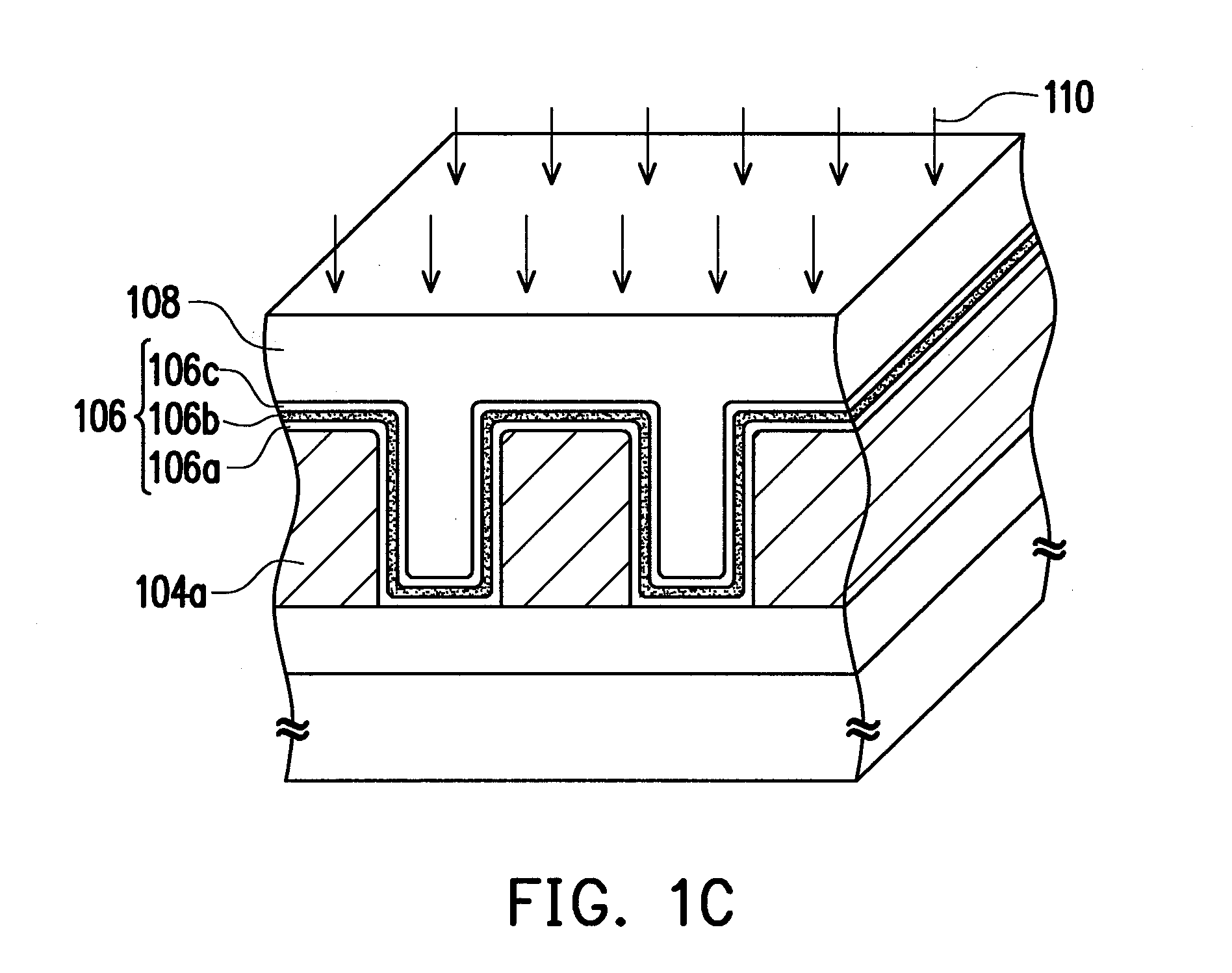
[0056]FIGS. 1A through 1F are a schematic three-dimensional view illustrating a method for forming a memory array according to one embodiment of the present invention. As shown in FIG. 1A, a substrate 100 is provided. The substrate 100 has a dielectric layer 102 formed thereon. The substrate 100 can be, for example but not limited to, a silicon substrate. The dielectric layer 102 can be, for example but not limited to, made of silicon oxide. The method for forming the dielectric layer 102 can be, for example but not limited to, chemical vapor deposition (CVD). Furthermore, a conductive layer 104 is formed on the dielectric layer 102. The conductive layer 104 can be, for example but not limited to, made of in-situ doped polysilicon. Alternatively, the method for forming the conductive layer 104 comprises steps of forming a polysilicon layer and then performing an ion implantation process for implanting ions into the polysilicon layer.
[0057]As shown in FIG. 1B, a patterning process is...
PUM
 Abstract
Description
Claims
Application Information