Systems and methods for stiction reduction in MEMS devices

a technology of mems devices and stiction reduction, which is applied in the direction of semiconductor devices, semiconductor/solid-state device details, electrical apparatus, etc., can solve the problems of unusable mems devices and unusable electrostatic effects, and achieve the effects of preventing stiction, preventing stiction, and improving the production yield of sensitive mems devices

Inactive Publication Date: 2010-07-22
HONEYWELL INT INC
View PDF18 Cites 20 Cited by
  • Summary
  • Abstract
  • Description
  • Claims
  • Application Information

AI Technical Summary

Benefits of technology

[0012]In yet further aspects of the invention, a method for preventing stiction between MEMS device components in an anodic bonding process includes bonding a first substrate cover to a first portion of a sensing or actuating element, disposing an antistiction element between a second portion of the sensing or actuating element and an interior surface of the second substrate cover, and bonding the first portion of the sensing or actuating element to a second substrate cover, such that the antistiction element prevents stiction of the second portion of the sensing element, when an electric potential is applied.
[0013]As will be readily appreciated from the foregoing summary, the invention provides means for improving the production yield of sensitive MEMS devices by deterring stiction between device components during anodic bonding.

Problems solved by technology

Unfortunately, when too high an electric potential is applied across a covering, an undesirable electrostatic effect occurs, which is commonly known as stiction.
This stiction can render a MEMS device unusable.

Method used


Image

  • Systems and methods for stiction reduction in MEMS devices
  • Systems and methods for stiction reduction in MEMS devices
  • Systems and methods for stiction reduction in MEMS devices

Examples


Embodiment Construction

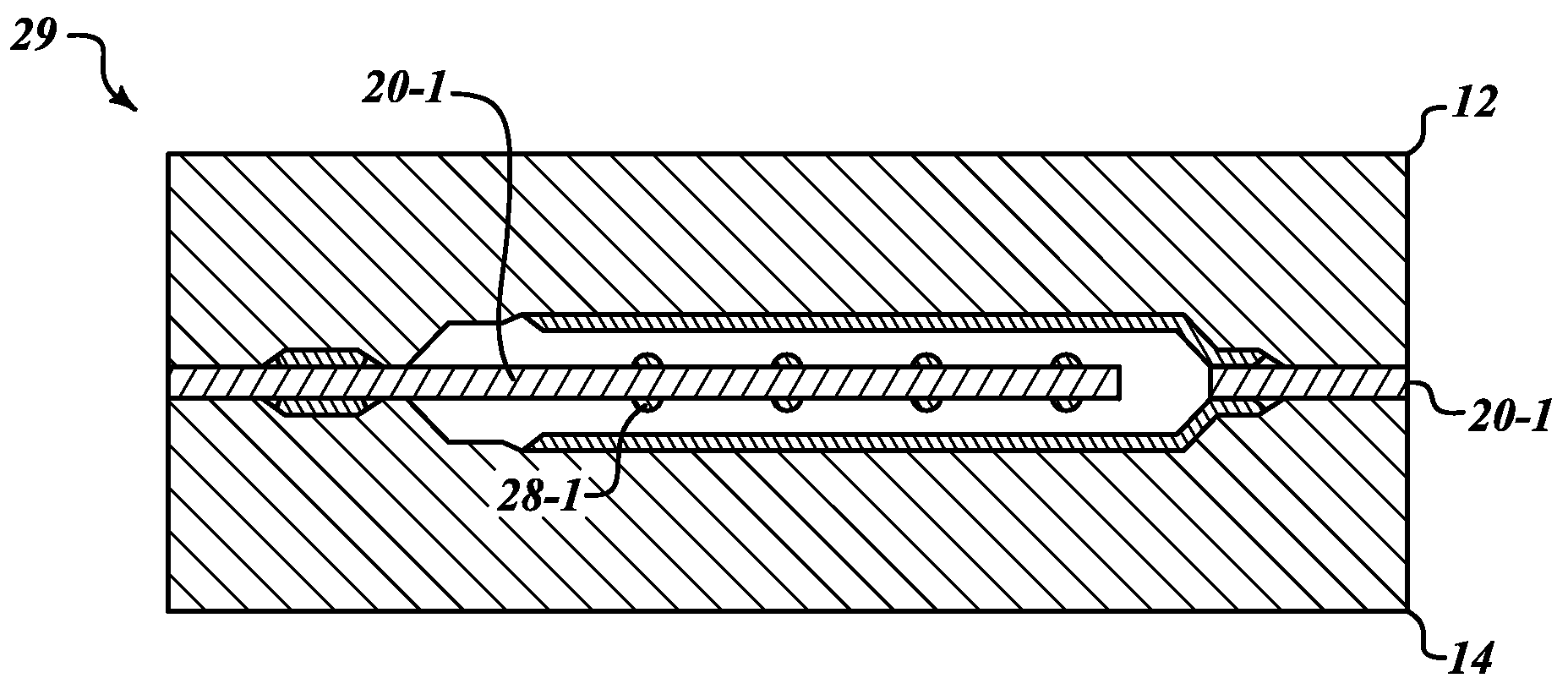
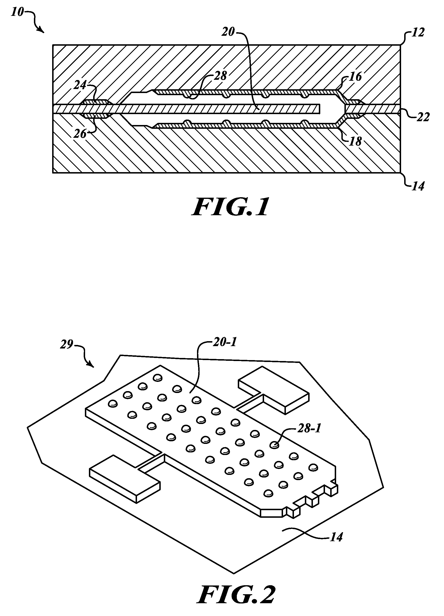
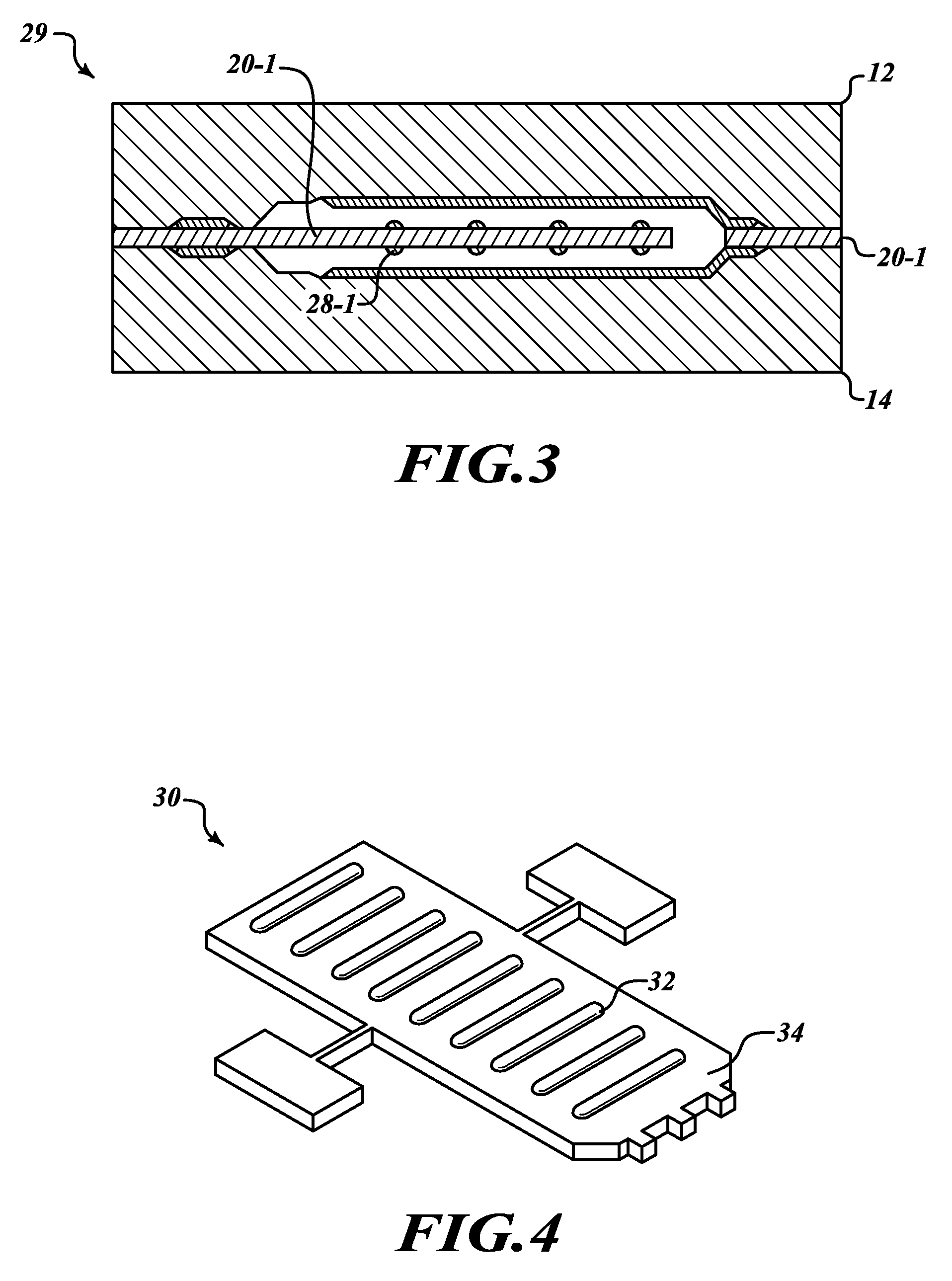
[0019]The present invention provides systems and methods for reducing stiction between elements of a microelectromechanical systems (MEMS) sensor or actuator device during anodic bonding. FIG. 1 illustrates a MEMS device 10 in accordance with an embodiment of the present invention. The components of the MEMS device 10 include: an upper substrate cover 12, a lower substrate cover 14, an upper conductor 16, a lower conductor 18, a sensing or actuating element 20 in a device layer 22, an upper anchor 24, a lower anchor 26, and one or more antistiction elements 28.

[0020]During fabrication of the MEMS device 10, the lower substrate cover 14 can be configured to include a lower conductor 18 that resides on an interior surface of the lower substrate cover 14. In an embodiment, the lower conductor 18 includes the antistiction elements 28. In accordance with a first bonding process, a single wafer substrate that includes the sensing or actuating element 20 in the device layer 22 are bonded t...


PUM


Abstract

Systems and methods for reducing stiction between elements of a microelectromechanical systems (MEMS) device during anodic bonding. The MEMS device includes a substrate cover with an optional conductor on its interior surface and the cover is anchored to a first portion of a sensing element. The MEMS device further includes a second portion of the sensing element separated from the substrate cover with a space and an antistiction element disposed between the second portion and cover. The antistiction element can be formed of a material type with high electrostatic resistance, to prevent stiction between MEMS device elements during anodic bonding.

Description

BACKGROUND OF THE INVENTION[0001]Certain microelectromechanical (MEMS) sensor devices include both an upper and a lower covering with a space-gap interposed therebetween. This space gap can contain a substrate wafer that acts as a sensing or actuating mechanism for the MEMS device. The gap is formed between recessed areas at the periphery of the upper and lower coverings, and the substrate wafer can be hermetically sealed between the two coverings in a very sensitive anodic bonding process.[0002]During an anodic bonding process, a secured substrate wafer is first bonded to the lower covering at raised contact regions at the covering's periphery edge. This process can involve the application of high temperatures and an electric potential of several hundred to a few thousand volts. Next, wafer elements that constrain device movement in a plane orthogonal to the covering are removed and the upper covering is similarly bonded to both the unsecured substrate wafer and the lower covering ...

Claims


Application Information

Patent Timeline
Patent Type & Authority Applications(United States)
IPC IPC(8): H01L23/44H01L21/02
CPCB81B3/001B81C2203/031
Inventor MILNE, CHRISRIDLEY, JEFF A.MAGENDANZ, GALENRUIZ, MARCOS DANIEL
Owner HONEYWELL INT INC
Why Eureka
Try Eureka