Liquid crystal display device, method of manufacturing the same and alignment layer composition for the liquid crystal display device

a liquid crystal display and alignment layer technology, which is applied in the manufacture of tubes/lamp screens, instruments, transportation and packaging, etc., can solve the problems of organic material decomposition and reliability degradation, the alignment layer composition may not be easily cured at the surface of the alignment layer, and the pre-images may not be uniform, so as to improve the aperture ratio and the response time, the effect of improving the display quality

Active Publication Date: 2010-07-22
SHENZHEN CHINA STAR OPTOELECTRONICS TECH CO LTD
View PDF12 Cites 54 Cited by
  • Summary
  • Abstract
  • Description
  • Claims
  • Application Information

AI Technical Summary

Benefits of technology

[0029]According to the present invention, the aperture ratio and the response time may be improved, and afterimages may be decreased, so that display quality may be improved. Thus,

Problems solved by technology

However, the RM may not be easily cured at a surface of the alignment layer, and the RM may remain in the liquid crystal layer.
Cured amounts of the RM are different from each other depending on their location so that the pre

Method used


Image

  • Liquid crystal display device, method of manufacturing the same and alignment layer composition for the liquid crystal display device
  • Liquid crystal display device, method of manufacturing the same and alignment layer composition for the liquid crystal display device
  • Liquid crystal display device, method of manufacturing the same and alignment layer composition for the liquid crystal display device

Examples


Embodiment Construction

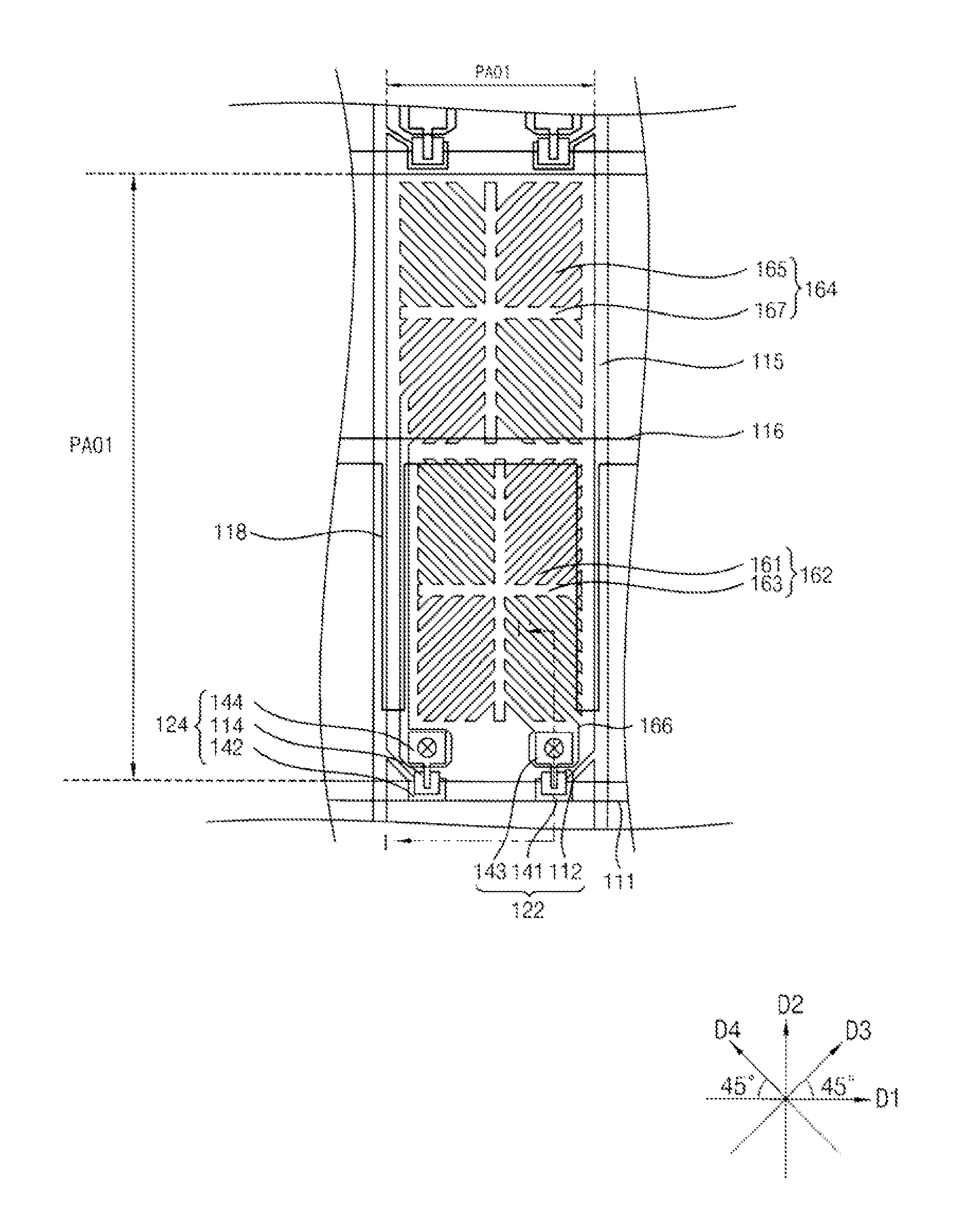
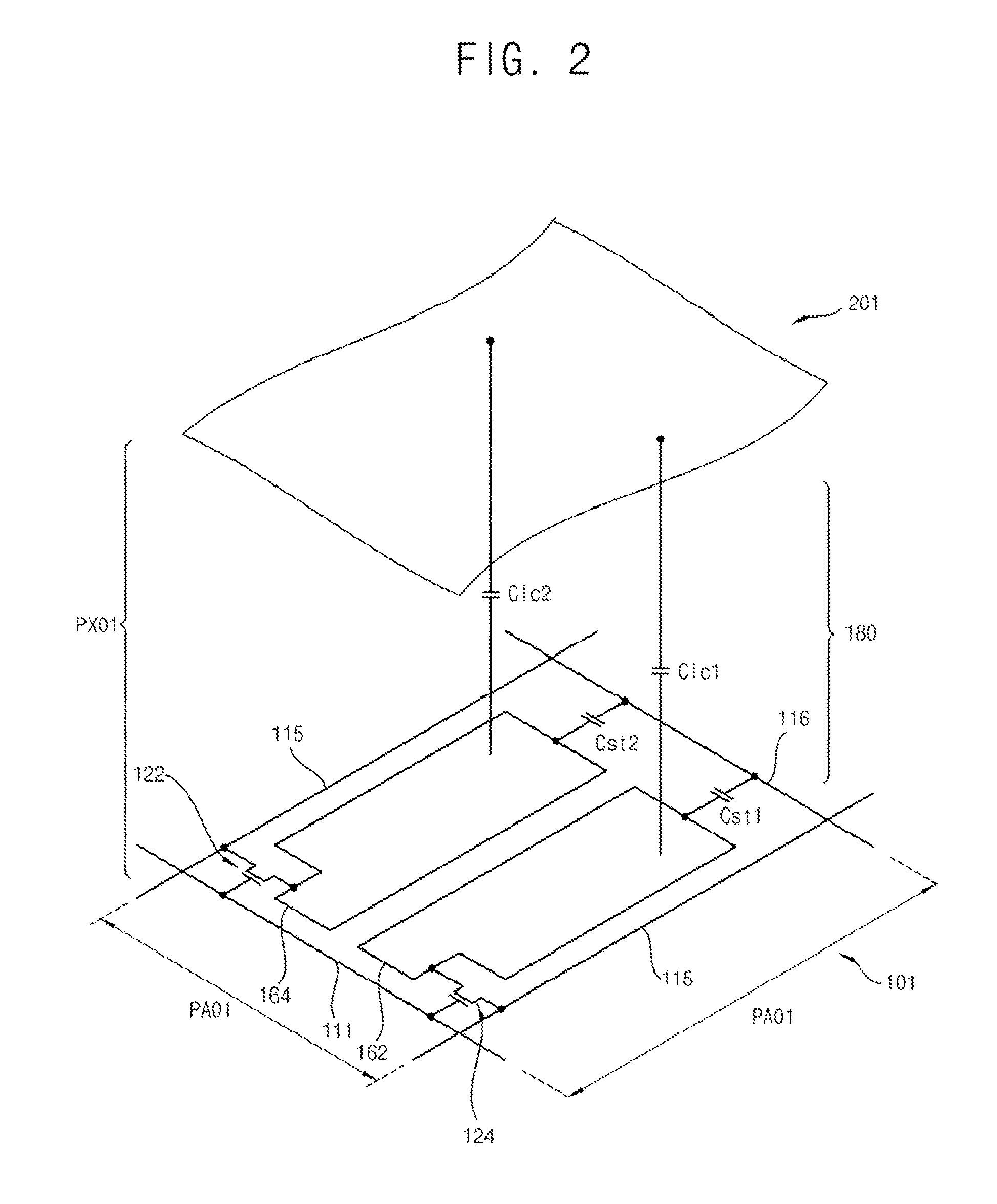
[0044]The present invention is described more fully hereinafter with reference to the accompanying drawings, in which embodiments of the present invention are shown. The present invention may, however, be embodied in many different forms and should not be construed as limited to the embodiments set forth herein. Rather, these embodiments are provided so that this disclosure will be thorough and complete, and will fully convey the scope of the present invention to those skilled in the art. In the drawings, the sizes and relative sizes of layers and regions may be exaggerated for clarity.

[0045]It will be understood that when an element or layer is referred to as being “on,”“connected to” or “coupled to” another element or layer, it can be directly on, connected or coupled to the other element or layer or intervening elements or layers may be present. In contrast, when an element is referred to as being “directly on,”“directly connected to” or “directly coupled to” another element or l...


PUM

PropertyMeasurementUnit
Structureaaaaaaaaaa
Electric potential / voltageaaaaaaaaaa
Areaaaaaaaaaaa

Abstract

A liquid crystal display device that includes an array substrate, an opposite substrate and a liquid crystal display layer is described. The array substrate includes a pixel electrode and a lower alignment layer. The pixel electrode has a plurality of slit portions extending in different directions. The lower alignment layer includes a reactive mesogen (RM) diamine is formed on the pixel electrode to induce an alignment direction of the liquid crystal molecules. An upper alignment layer is formed on a common electrode of the opposite substrate. The RM is cured at surfaces of the lower and upper alignment layers in response to ultraviolet (UV) light, so that liquid crystal molecules have a pretilt angle. Therefore, the aperture ratio and the response time may be improved, and afterimages may be decreased, so that display quality may be improved.

Description

CROSS REFERENCE TO RELATED APPLICATION[0001]This application claims priority under 35 U.S.C. §119 to Korean Patent Application No. 2009-4174, filed on Jan. 19, 2009 in the Korean Intellectual Property Office (KIPO), the contents of which are herein incorporated by reference in their entirety.BACKGROUND OF THE INVENTION[0002]1. Field of the Invention[0003]The present invention relates to a liquid crystal display (LCD) device, a method of manufacturing the LCD device and an alignment layer composition used for the LCD device. More particularly, the present invention relates to an LCD device capable of enhancing display quality by improving the viewing angle and the response time, a method of manufacturing the LCD device and an alignment layer composition used for the LCD device.[0004]2. Description of the Related Art[0005]Generally, in a liquid crystal display (LCD) device, a voltage is applied to an electric field generating electrode to provide the liquid crystal layer with an elect...

Claims


Application Information

Patent Timeline
IPC IPC(8): G02F1/1337G02F1/13C09K19/56
CPCG02F1/133707G02F1/133723G02F1/133788G02F2001/133726Y10T428/1005Y10T428/1023H01J9/205H01J9/233Y10T428/10C09K19/56C09K2323/00C09K2323/02C09K2323/027G02F1/133726C08J5/18G02F1/1337
Inventor OH, KEUN-CHANLYU, JAE-JINSOHN, JI-WONCHO, SEON-AH
Owner SHENZHEN CHINA STAR OPTOELECTRONICS TECH CO LTD
Why Eureka
Try Eureka