Resin sealing method of semiconductor device

a sealing method and semiconductor technology, applied in semiconductor devices, semiconductor/solid-state device details, electrical devices, etc., can solve problems such as reducing yield, defective semiconductor devices of most or all of the semiconductor devices on the support plate, and misregistration of some semiconductor devices

Active Publication Date: 2010-07-22
SHINKO ELECTRIC IND CO LTD
View PDF2 Cites 47 Cited by
  • Summary
  • Abstract
  • Description
  • Claims
  • Application Information

AI Technical Summary

Benefits of technology

[0009]It is therefore an object of the invention to solve problems of a conventional resin sealing method of a semiconductor device wherein misregistration of semiconductor devices is caused easily to occur by the fluid power of a seal resin when the semiconductor devices adhered to predetermined positions of an adhesive layer formed on one face side of a

Problems solved by technology

Thus, it has become evident that there is a problem in that when the semiconductor devices are sealed with resin, misregistration of some semiconductor devices occurs because of a seal resin flow.
Such misregis

Method used


Image

  • Resin sealing method of semiconductor device
  • Resin sealing method of semiconductor device
  • Resin sealing method of semiconductor device

Examples


first embodiment

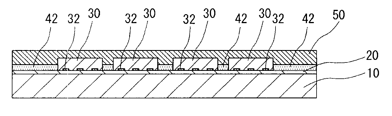
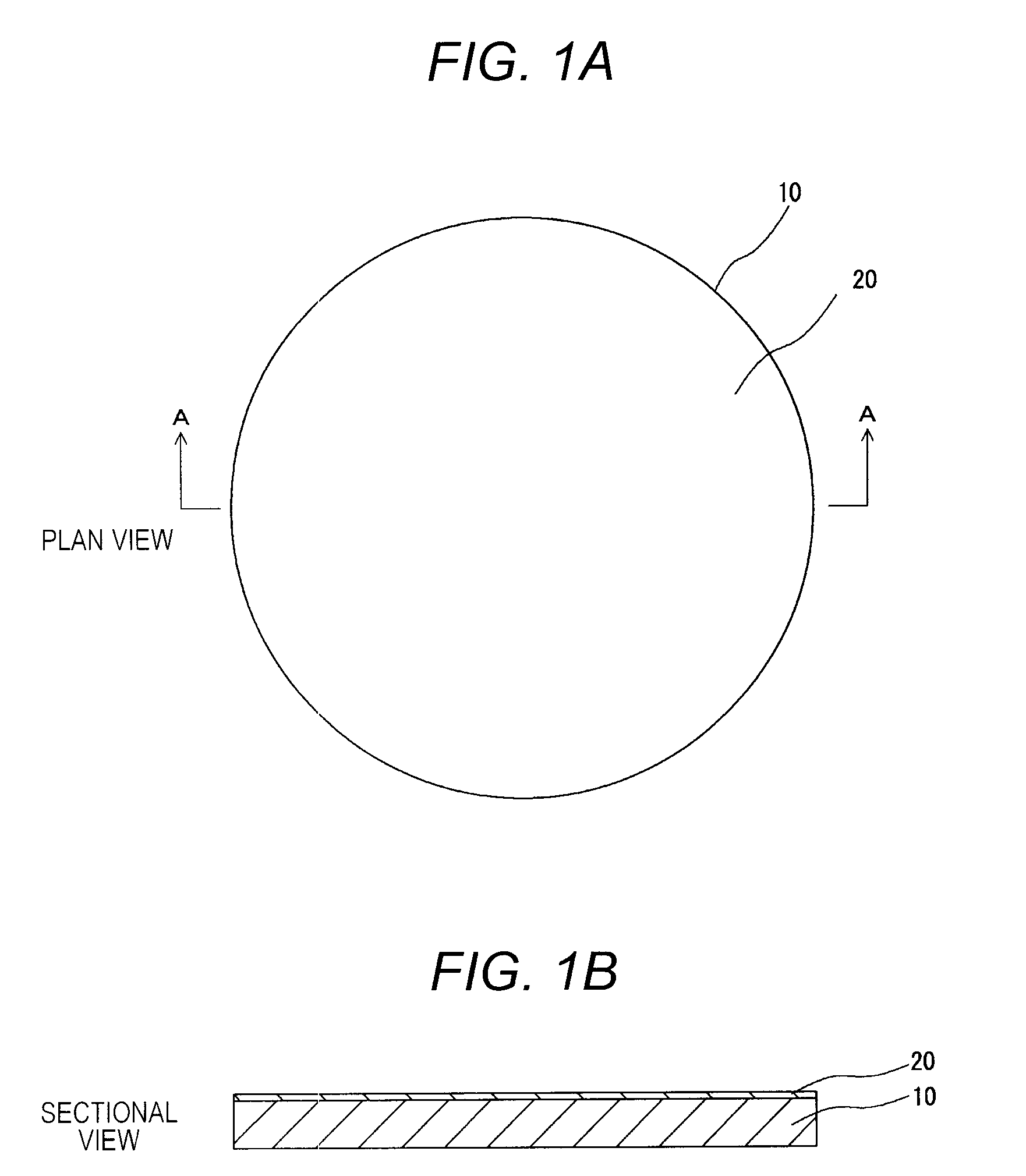
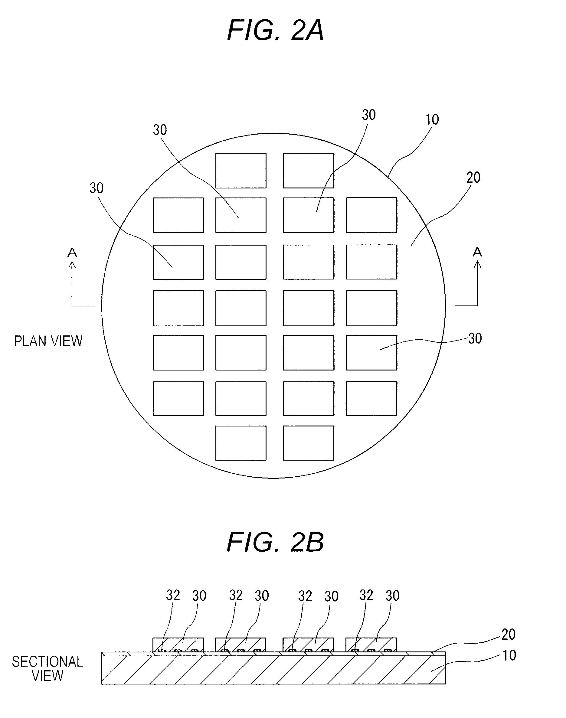
[0063]A resin sealing method of a semiconductor device according to a first embodiment of the invention will be discussed. FIGS. 1A to 3B are plan views and sectional views taken on line A-A to show the state in each step when semiconductor devices are sealed with resin according to the first embodiment of the invention. FIGS. 4A to 4D are sectional views taken on line A-A in FIG. 3A when the semiconductor devices are sealed with second seal resin. FIGS. 5A to 5F are sectional views to show the state of each step after FIG. 4D. The cross-sectional positions in FIG. 5A to 5F are the same as those in FIG. 4A to 4D.

[0064]To begin with, as shown in FIGS. 1A and 1B, an adhesive layer 20 to adhere each semiconductor device 30 to a support body 10 made of a thin copper plate is formed. An epoxy-based adhesive is applied or an adhesive sheet is put on the upper face of the support body 10, whereby the adhesive layer 20 can be formed. In the embodiment, the plate thickness of the support bod...

second embodiment

[0074]A second embodiment of the invention is characterized by disposition of a frame body 12 to prevent a liquid resin 40 which becomes a first seal resin 42 for sealing a part of each semiconductor device 30 to fix the semiconductor device 30 from flowing out from the seal area on a support body. FIGS. 6A, 6B, 7A and 7B are plan views and sectional views taken on line A-A to describe sealing the semiconductor devices with resin according to the second embodiment of the invention. FIGS. 8A to 8F are sectional views to show the state in each step after FIG. 7B. The cross-sectional positions in FIGS. 8A to 8F are the same as those in FIGS. 6A, 6B, 7A and 7B.

[0075]In the second embodiment, first, an adhesive layer 20 is formed on the upper face of a support body 10 as with the first embodiment. Then, the above-mentioned frame body 12 is disposed as shown in FIGS. 6A and 6B before the semiconductor devices 30 are adhered to the adhesive layer 20. The frame body 12 is made of a metal ma...

third embodiment

[0078]FIG. 9A is a plan view to show a state when a resin sealing method of a semiconductor device is executed in a third embodiment of the invention. FIGS. 10A to 10F are sectional views taken on line A-A to show the state when the resin sealing method of the semiconductor device is executed in the third embodiment of the invention.

[0079]The third embodiment is characterized by the fact that stoppers 24 are formed at positions along the periphery of semiconductor devices 30 as misregistration prevention means (fixing means) of the semiconductor devices 30 adhered to an adhesive layer 20 formed on the upper face of a support body 10.

[0080]First, the adhesive layer 20 is formed on the upper face of the support body 10 and a frame body 12 and the semiconductor devices 30 are positioned and are adhered to the adhesive layer 20 as in the second embodiment. After the semiconductor devices 30 are adhered to the adhesive layer 20, laser light irradiation means (not shown) forms stopper rec...


PUM


Abstract

A resin sealing method of a semiconductor device includes: positioning semiconductor devices at predetermined positions of an adhesive layer formed on a support body and adhering the semiconductor devices thereto, sealing a part of each of the semiconductor devices with resin by curing a first seal resin in a fluidization state so as to fix the semiconductor devices adhered to the predetermined positions of the adhesive layer formed on the support body, setting the semiconductor devices fixed to the predetermined positions of the adhesive layer formed on the support body in a mold and sealing the exposure parts of the semiconductor devices exposed from the first seal resin with a second seal resin, and removing the support body and the adhesive layer from the semiconductor devices sealed with the resin.

Description

CROSS-REFERENCE TO RELATED APPLICATION[0001]This application is based on and claims priority under 35 U.S.C. §119 from Japanese Patent Application No. 2009-003000 filed on Jan. 16, 2009.BACKGROUND OF THE INVENTION[0002]1. Technical Field[0003]This invention relates to a resin sealing method of a semiconductor device and more particularly to a resin sealing method of a semiconductor device for making it possible to prevent misregistration of the semiconductor device at the resin sealing time when the semiconductor device disposed at a predetermined position of a support plate is sealed with a resin.[0004]2. Related Arts[0005]After each of semiconductor devices each formed with electrode terminals on one side is positioned and is disposed with the electrode terminals aimed at an adhesive layer applied onto a support body, an opposite side of each of the semiconductor devices is sealed with a seal resin in a collective manner. This method is known as a molding method. Representative mo...

Claims


Application Information

Patent Timeline
IPC IPC(8): H01L21/56
CPCH01L21/561H01L21/565H01L23/3128H01L23/5389H01L24/96H01L24/97H01L25/0655H01L2224/04105H01L2224/20H01L2224/92H01L2224/97H01L2924/01029H01L2924/01075H01L2924/01079H01L2924/15174H01L2924/15311H01L2224/96H01L2224/82H01L2924/01005H01L2924/01006H01L2924/01033H01L23/28H01L23/488H01L24/19H01L2224/12105H01L2224/0401H01L23/3135H01L21/568H01L2224/24137H01L2924/181H01L2924/00H01L2924/3511H01L2924/12042H01L2924/19107
Inventor CHINO, TERUAKI
Owner SHINKO ELECTRIC IND CO LTD
Why Eureka
Try Eureka