Implementing Enhanced SRAM Stability and Enhanced Chip Yield With Configurable Wordline Voltage Levels

a wordline voltage and stability technology, applied in the field of data processing, can solve the problems of increasing the variation of static random access memory (sram) cells, reducing yield, and difficulty in balancing the conflicting cell tuning requirements for read stability and writeability

Active Publication Date: 2010-07-29
MARVELL ASIA PTE LTD
View PDF2 Cites 12 Cited by
  • Summary
  • Abstract
  • Description
  • Claims
  • Application Information

AI Technical Summary

Benefits of technology

[0010]In accordance with features of the invention, the SRAM circuit includes a plurality of wordline voltage control latches having an ABIST interface for running ABIST tests and an input for receiving the wordline voltage level setting. The plurality of wordline voltage control latches provides a respective gate input to weak N-channel field effect transistors (NFETs) implementing the wordline voltage pulldown devices.

Problems solved by technology

As technology scales, static random access memory (SRAM) cell variation is becoming increasingly problematic.
In high speed memories, balancing the conflicting cell tuning requirements for read stability and writeability is also increasingly difficult.
Due to the sensitivity of the SRAM designs, process variation can greatly reduce yields.
Variation in dopant levels can increase or decrease device threshold voltages and skew the sensitive device strength ratios in the SRAM cell.
This variation can cause the SRAM cell to be unstable or unwriteable.
The SRAM cell can become unstable when process varies such that the pass gate voltage threshold (Vt) is decreased.

Method used


Image

  • Implementing Enhanced SRAM Stability and Enhanced Chip Yield With Configurable Wordline Voltage Levels
  • Implementing Enhanced SRAM Stability and Enhanced Chip Yield With Configurable Wordline Voltage Levels
  • Implementing Enhanced SRAM Stability and Enhanced Chip Yield With Configurable Wordline Voltage Levels

Examples


Embodiment Construction

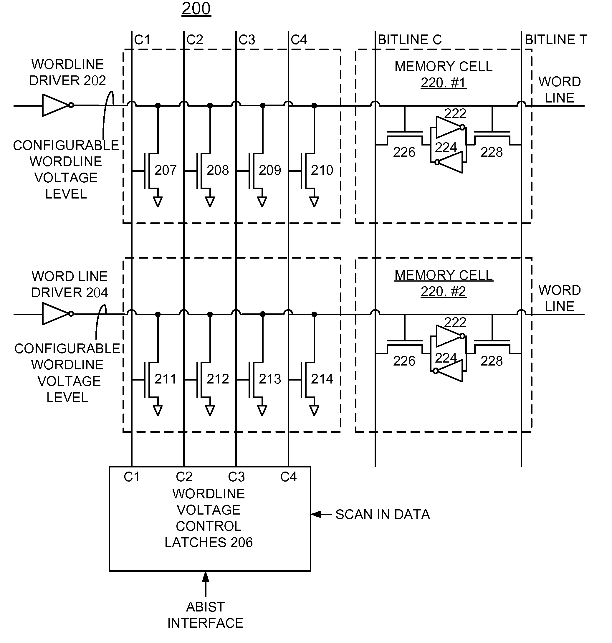
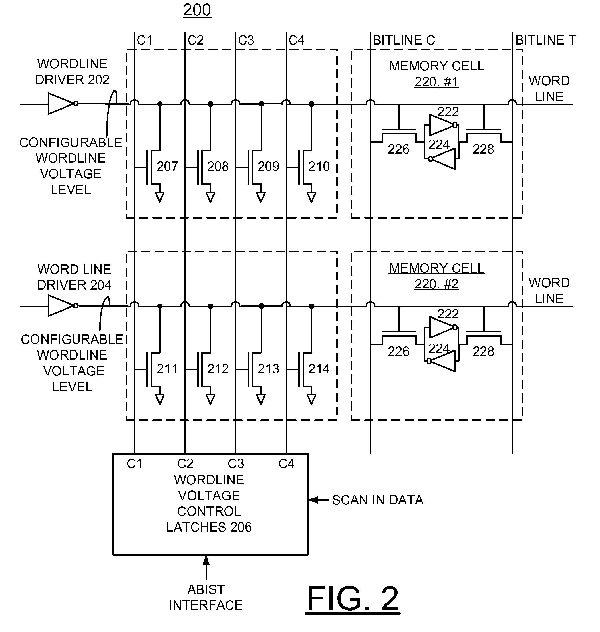
[0015]In accordance with features of the invention, a static random access memory (SRAM) circuit to adjust wordline voltage level and an Array Built In Self Test (ABIST) method using this circuit to reduce SRAM cell stability fails are provided. This SRAM circuit and ABIST method improves chip yields by correcting for process variation after manufacturing. The SRAM circuit and ABIST method adjusts the sensitive SRAM cell current ratio of pass gate to pulldown device via a configurable wordline voltage level.

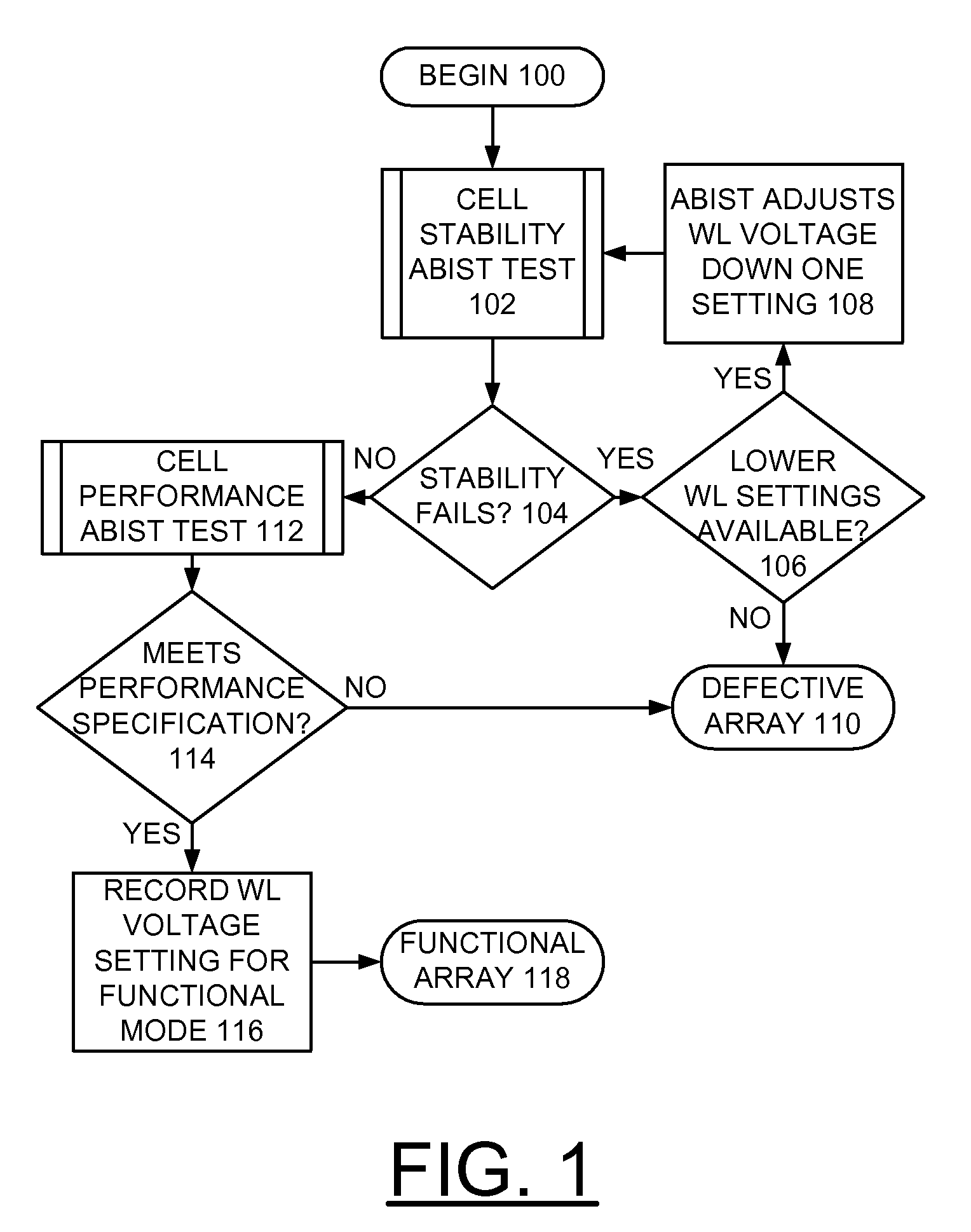
[0016]Having reference now to the drawings, in FIG. 1, there are shown exemplary steps of an array built-in self-test (ABIST) method in accordance with the preferred embodiment starting at a block 100. The ABIST method is provided using a static random access memory (SRAM) circuit, for example, as illustrated and described with respect to FIG. 2.

[0017]Cell stability ABIST patterns are run starting with a maximum wordline voltage as indicated at a block 102. Checking for any stabi...


PUM


Abstract

An array built in self test (ABIST) method and circuit for implementing enhanced static random access memory (SRAM) stability and enhanced chip yield using configurable wordline voltage levels, and a design structure on which the subject circuit resides are provided. A wordline is connected to a SRAM memory cell. A plurality of wordline voltage pulldown devices is connected to the wordline. A respective wordline voltage control input signal is applied to each of the plurality of wordline voltage pulldown devices to selectively adjust the voltage level of the wordline.

Description

FIELD OF THE INVENTION[0001]The present invention relates generally to the data processing field, and more particularly, relates to an array built in self test (ABIST) method and circuit for implementing enhanced static random access memory (SRAM) stability and enhanced chip yield using configurable wordline voltage levels, and a design structure on which the subject circuit resides.DESCRIPTION OF THE RELATED ART[0002]As technology scales, static random access memory (SRAM) cell variation is becoming increasingly problematic. In high speed memories, balancing the conflicting cell tuning requirements for read stability and writeability is also increasingly difficult.[0003]Due to the sensitivity of the SRAM designs, process variation can greatly reduce yields. Variation in dopant levels can increase or decrease device threshold voltages and skew the sensitive device strength ratios in the SRAM cell. This variation can cause the SRAM cell to be unstable or unwriteable.[0004]The SRAM ce...

Claims


Application Information

Patent Timeline
Patent Type & Authority Applications(United States)
IPC IPC(8): G11C11/00G11C29/00
CPCG11C8/08G11C11/41G11C11/413G11C11/419G11C2029/5002G11C29/021G11C29/028G11C29/12005G11C29/50G11C29/02
Inventor BEHRENDS, DERICK GARDNERHEBIG, TRAVIS REYNOLDNELSON, DANIEL MARKSMITH, JESSE DANIEL
Owner MARVELL ASIA PTE LTD
Why Eureka
Try Eureka