

Method of fabricating semiconductor device
a semiconductor and device technology, applied in the direction of semiconductor devices, basic electric elements, electrical equipment, etc., can solve the problems of more microscopic patterns than resolution limitations, and achieve the effects of higher etch selectivity, higher etch selectivity, and higher etch selectivity
- Summary
- Abstract
- Description
- Claims
- Application Information
AI Technical Summary
Benefits of technology
Problems solved by technology
Method used
Image

Examples
first embodiment
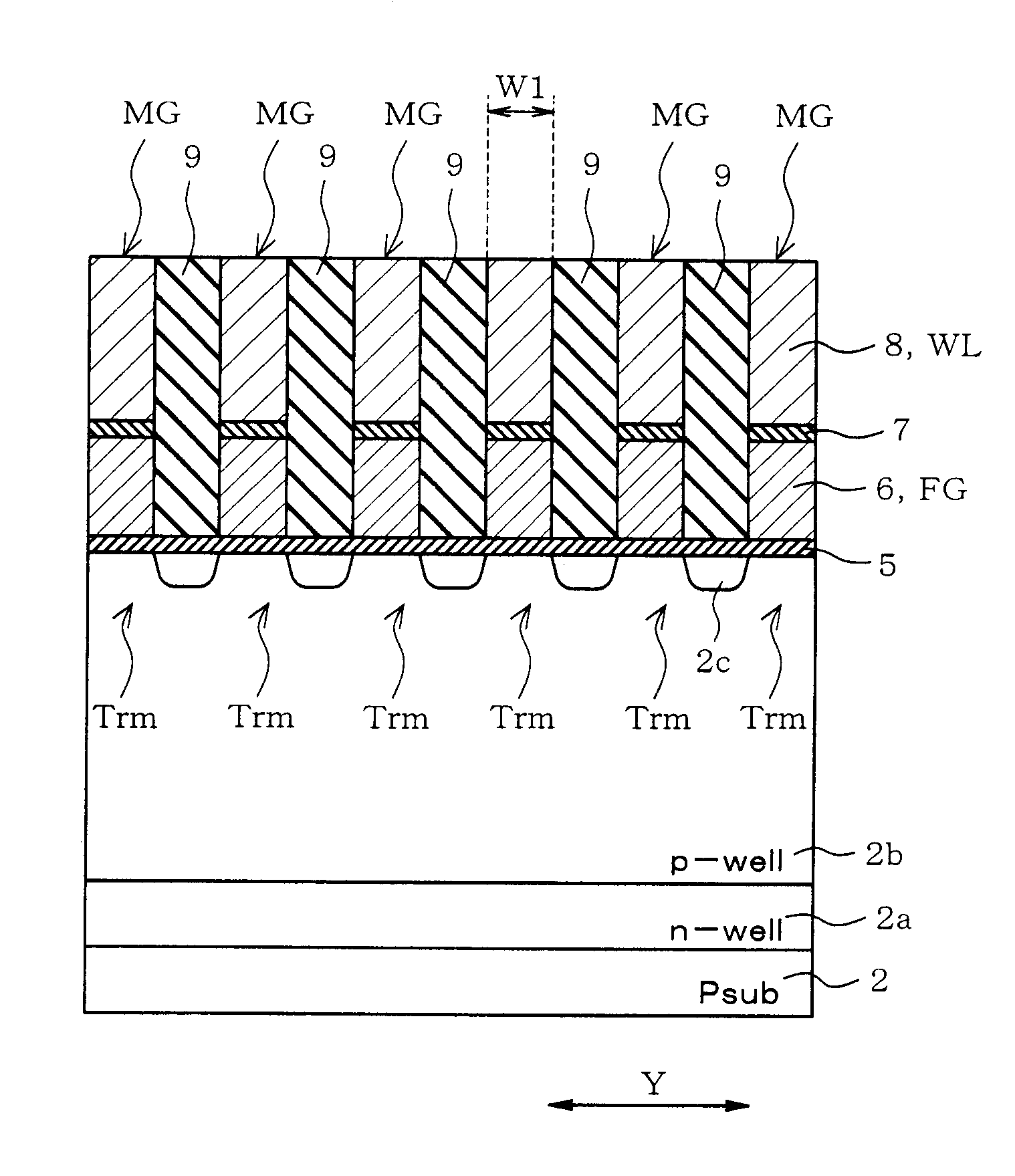
[0021]A first embodiment will be described with reference to FIGS. 1 to 17B. The embodiment is directed to a process of fabricating a NAND flash memory. In the following description, identical or similar parts are labeled by the same reference symbols. The drawings typically illustrate the embodiments, and the relationship between a thickness and planar dimension, layer thickness ratio and the like differ from respective natural dimensions.
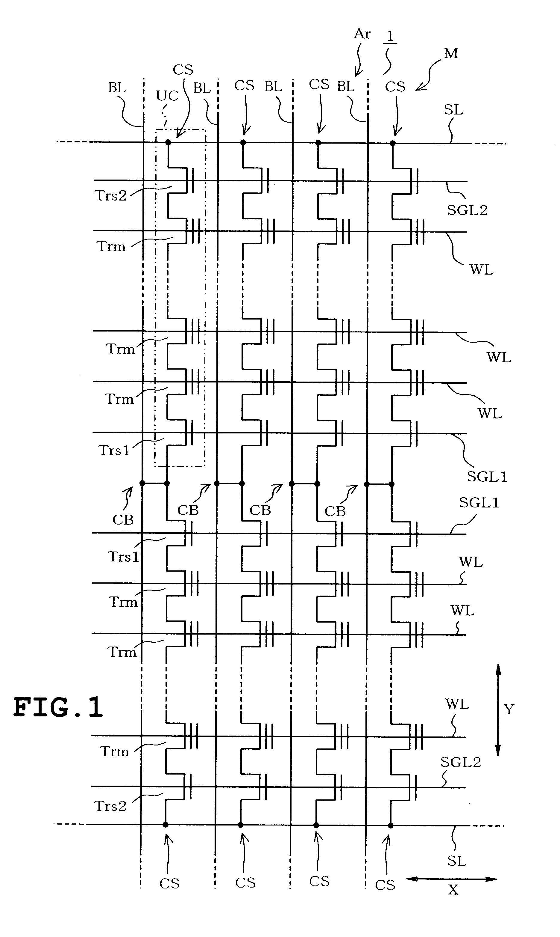
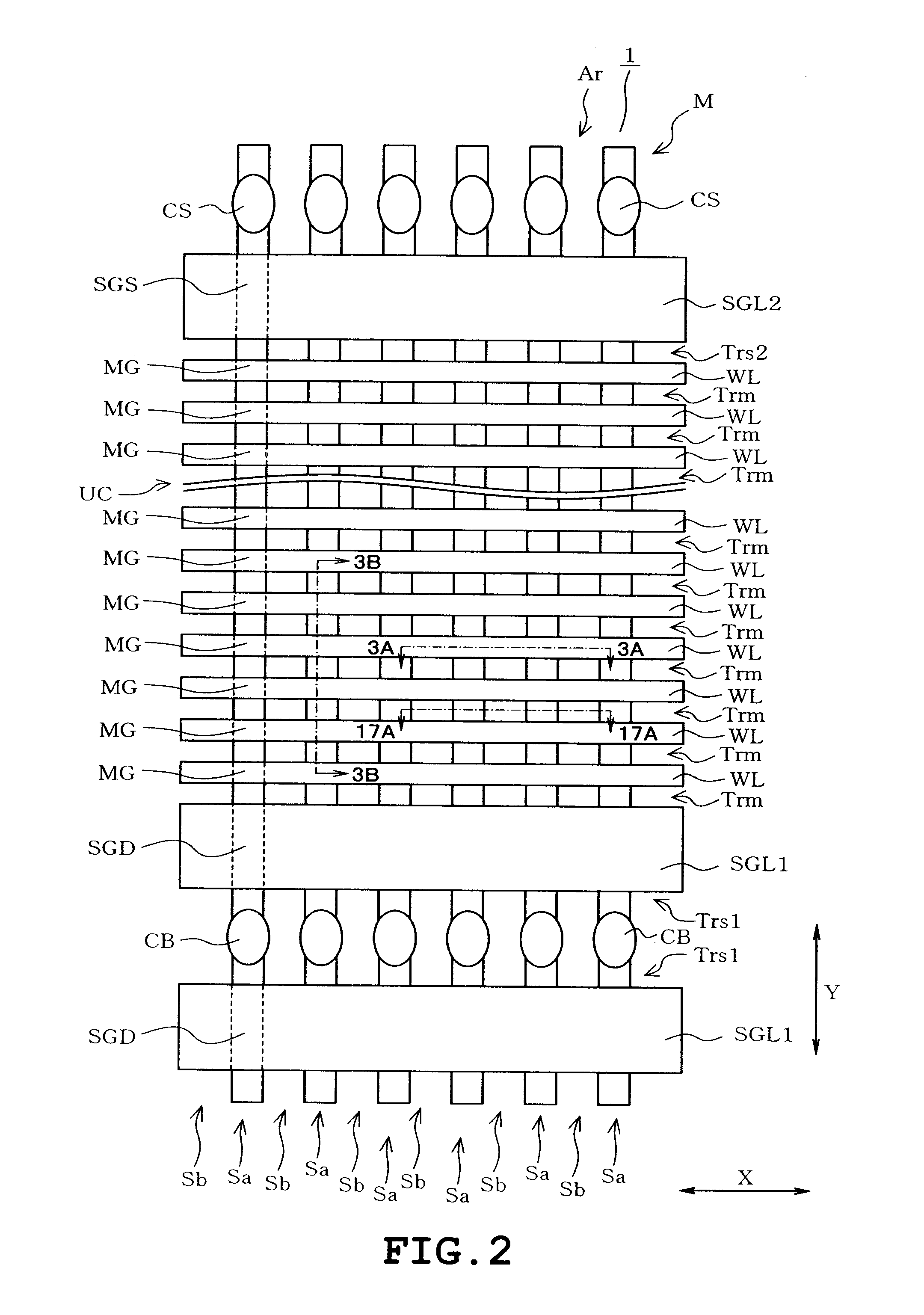
[0022]A NAND flash memory device 1 as a semiconductor device comprises a memory cell region M and a peripheral circuit region (not shown) . The memory cell region M is provided with a memory cell array Ar including a number of memory cell transistors Trm arranged in a matrix. The peripheral circuit region is provided with peripheral circuits (not shown) to drive the memory cell transistors Trm.
[0023]FIG. 1 shows an equivalent circuit of a part of the memory cell array in the flash memory. As shown, the memory cell array Ar includes NAND cell units...
third embodiment
[0067] the microstructurization in the X direction can be achieved since the fabrication method is applied to the forming of the element isclation trenches 3.
[0068]The foregoing embodiments are not restrictive and can be modified or expanded as follows. Although the foregoing embodiments are applied to the flash memory 1, any other semiconductor device necessitating the microstructurization may be embodied. Furthermore, although the foregoing embodiments are directed to the respective forms of fabrication process, one or more embodiments may be directed to a step of forming trenches in an interlayer insulating film or a step of forming bit lines.
[0069]Although the p-type silicon substrate formed with the wells 2a and 2b is applied to the semiconductor substrate 2 in the foregoing embodiments, a n-type silicon substrate having a surface layer formed with p-wells may be employed, instead. Furthermore, the X and Y directions may be perpendicular to each other in the upper surface of th...
PUM
 Abstract
Description
Claims
Application Information