Method of mounting LED chip

a technology of led chips and mounting parts, which is applied in the direction of light and heating equipment, semiconductor devices for light sources, solid-state devices, etc., can solve the problems of excessive thermal resistance of luminaires, limited light output, and residues on mounting parts, so as to prevent excessive extension of eutectic bonds, improve the uniformity of metal layers, and suppress the generation of voids inside metal layers

Inactive Publication Date: 2010-08-19
PANASONIC CORP
View PDF6 Cites 15 Cited by
  • Summary
  • Abstract
  • Description
  • Claims
  • Application Information

AI Technical Summary

Benefits of technology

[0010]The present invention relates to the method of mounting the LED chip to a dielectric substrate by way of a metallic bond. The method in the present invention comprises a step of forming a metal ground layer on a top surface of the dielectric substrate; a step of forming a first metal layer of an eutectic alloy on a bottom surface of the LED chip; a step of providing a second metal layer having the same metal component as the first metal layer, to the top surface of the metal ground layer; and a step of heating the dielectric substrate at its bottom surface remote from the metal ground layer to melt the second metal layer, subsequently bonding the first metal layer with the second metal layer. The method in the present invention enables to suppress the void-generation inside metal layers without use of flux.
[0011]The second metal layer is preferably formed of an eutectic alloy containing the same metals as the first metal layer, and further preferably has the same metal composition ratio as the first metal layer so as to improve the uniformity of the metal layers. Instead, the second metal layer preferably has a metal composition ratio different from that of the first metal layer, and a melting point higher than the first metal layer, for being easily bonded with the first metal layer. Each of the first metal layer and the second metal layer is preferably formed of an eutectic Au—Sn alloy. The metal ground layer preferably has an Au layer at its top. The second metal layer is preferably formed over a top of the Au layer with a Pt layer interposed therebetween. Each of the Pt layer and the second metal layer preferably has the same plane size as the LED chip. The method in the present invention is capable of generating the eutectic bond of the AuSn eutectic alloy as well as preventing an excessive extension of the eutectic bond.
[0012]The second metal layer preferably includes a plurality of metal layers each containing any one of metals forming said first metal layer. In addition, it is preferable that the first metal layer is made of an eutectic Au—Sn alloy, and the metal ground layer has an Au layer at its top. It is preferable that a plurality of the metal layers forming the second metal layer include an Sn layer formed on the Au layer of the metal ground layer, and an Au layer formed on the Sn layer. The method in the present invention is capable of generating the eutectic bond of AuSn eutectic alloy as well as preventing an excessive extension of the eutectic bond.

Problems solved by technology

As a result, this luminaire may suffer from an excessive thermal resistance between the LED chip and the main body.
As a result, this light emitting device may give a limited light output.
But, this process needs the use of flux, possibly leaving residues on the mounting member.
Besides, the eutectic bond may undergo ununiform temperature due to a partial sudden boiling when the melted eutectic alloy layer comes to contact with the patterned conductor, suffering from void-generation inside the eutectic bond, and eventually increasing the thermal resistance between the LED chip and the mounting member.
In addition, it is difficult to suitably control temperature and time of heating the melted eutectic alloy layer in accordance with thermal resistance of the LED chip.

Method used


Image

  • Method of mounting LED chip
  • Method of mounting LED chip
  • Method of mounting LED chip

Examples


Embodiment Construction

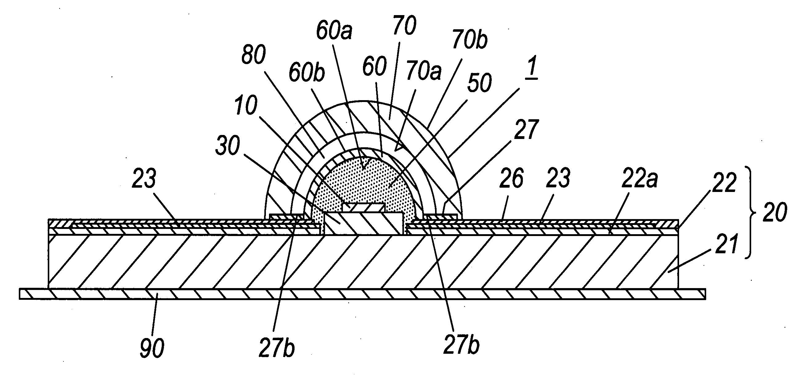
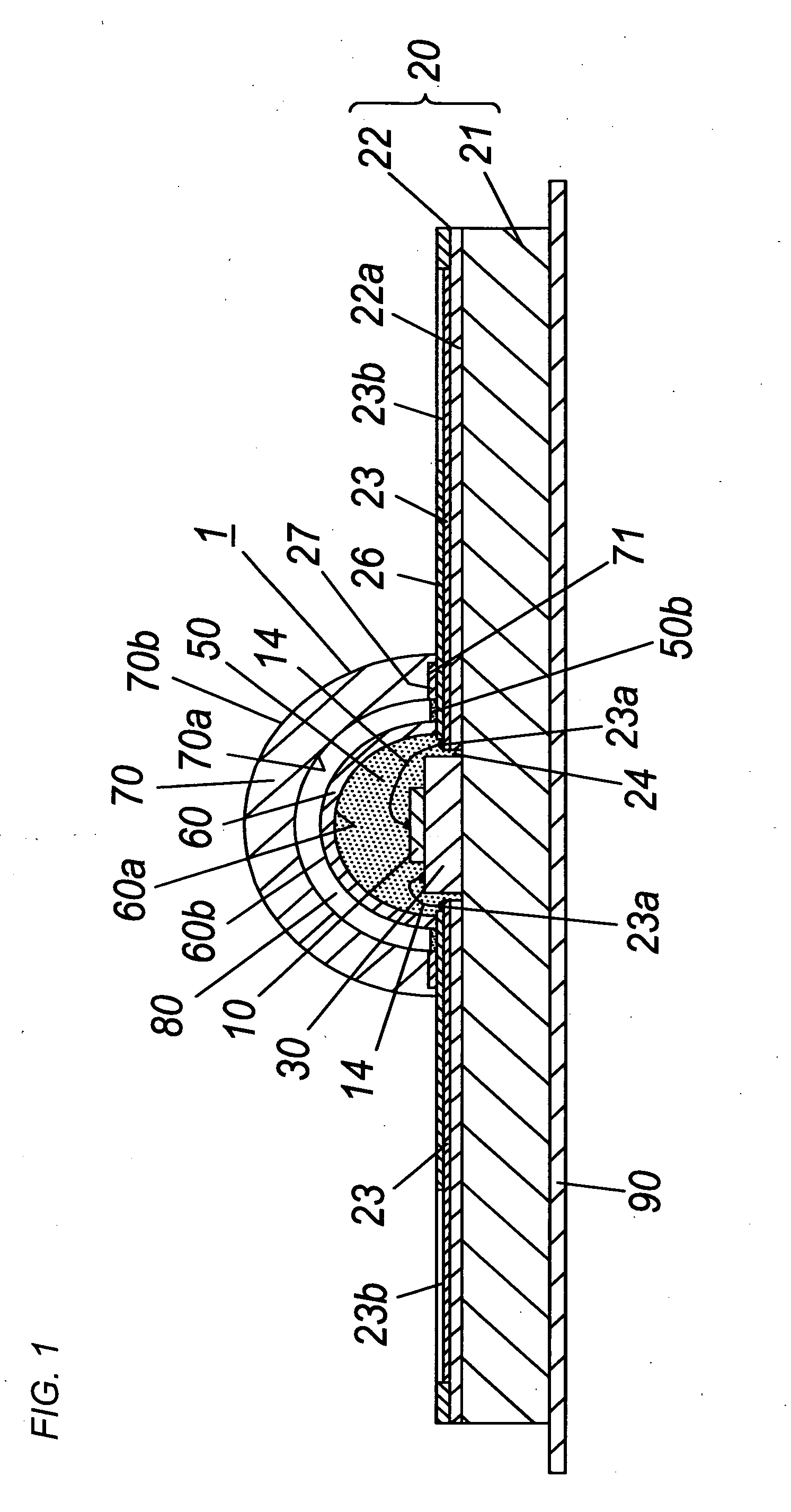
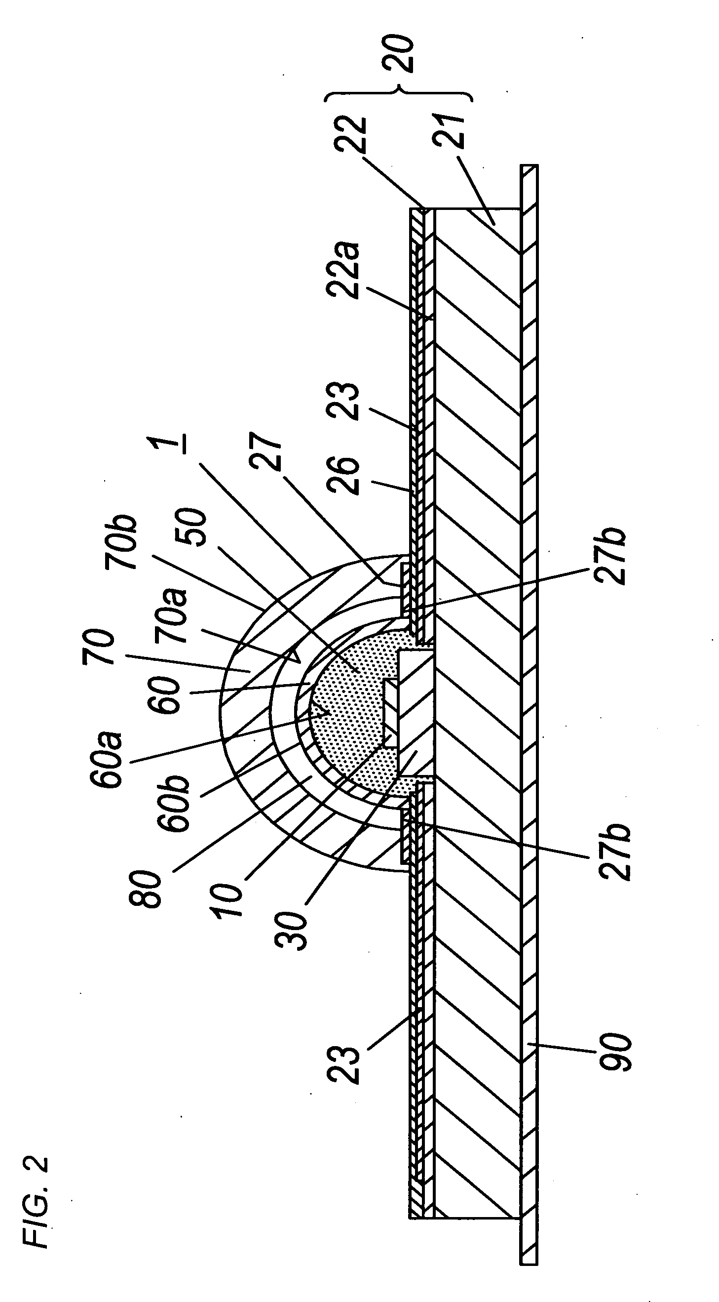
[0021]Hereafter, explanations are given as to a light emitting device in an embodiment, with reference to FIGS. 1 to 8.

[0022]As shown in FIGS. 1 and 2, the light emitting device 1 in this embodiment comprises an LED chip 10, a mounting substrate 20 shaped into a rectangular plate which holds the LED chip 10, a′dome-shaped optical member 60 made of a light-transmissive material, a light-transmissive elastic encapsulation resin 50, and a dome-shaped color conversion member 70. The mounting substrate 20 is provided at its top surface with a ring gate 27. The ring gate 27 is formed outside of the optical member 60 to protrude from the top surface of the mounting substrate. The mounting substrate 20 is provided at its top surface with the LED chip 10 and a patterned conductor 23 which supplies electric power to the LED chip 10. The encapsulation resin 50 is filled in a space confined between the optical member 60 and the mounting substrate 20 for encapsulating therewith the LED chip 10 a...


PUM

PropertyMeasurementUnit
temperatureaaaaaaaaaa
thicknessesaaaaaaaaaa

Abstract

A method of mounting an LED chip, which is intended to suppress void-generation inside an eutectic bonding without use of flux. This method includes a step of eutectically bonding a first metal layer (e.g., AuSn layer) on a rear surface of the LED chip, with a metal ground layer on a dielectric substrate (mounting member). This method includes a step of providing a second metal layer having the same metal component as the first metal layer, to the top surface of the metal ground layer on a dielectric substrate; and subsequently connecting the LED chip and the dielectric substrate by way of eutectically bond while the dielectric substrate is heated at its bottom surface remote from the metal ground layer to melt the second metal layer by heat source (heater or the like).

Description

TECHNICAL FIELD[0001]This invention relates to a method of mounting LED chip.BACKGROUND ART[0002]Many studies have been widely carried out to develop light emitting device which radiates a mixed-color light and luminaire using the light emitting device so far. The light emitting device includes an LED chip and a phosphor. (e.g., Reference 1) The phosphor acts as a wavelength conversion member which is excited by a light emitted from LED chip and emits a light of color different from the luminescent color of the LED. The light emitting device is capable of radiating a light of mixed-color which is different from the luminescent color of LED, when including the phosphor and the LED chip. For example, it is known that the blue-color or UV LED chip can be combined with the phosphor to give a light emitting device which radiates a white-color light (white-color luminescent spectrum).[0003]For example, the light emitting device radiating white-color light is combined with each other for b...

Claims


Application Information

Patent Timeline
Patent Type & Authority Applications(United States)
IPC IPC(8): H01L33/48H01L33/32H01L33/56H01L33/62
CPCF21K9/00H01L2924/0001H01L33/40H01L33/62H01L2224/48091H01L33/32H01L2924/0133H01L2924/0132H01L24/29H01L24/45H01L24/83H01L2224/29144H01L2224/2919H01L2224/32227H01L2224/45124H01L2224/45144H01L2224/48227H01L2224/48465H01L2224/73265H01L2224/83193H01L2224/83815H01L2224/92247H01L2924/01005H01L2924/01006H01L2924/01073H01L2924/01074H01L2924/01322H01L2924/014H01L2924/0665H01L2924/3656H01L2924/12041H01L2224/29386H01L2224/2929H01L2924/01029H01L2924/01028H01L2924/01014H01L2924/01013H01L2924/00013H01L2224/29111H01L2924/1579H01L2924/00014H01L2924/0105H01L2924/05442H01L2924/05432H01L2924/00H01L2924/01047H01L2924/01079H01L2224/29099H01L2224/29199H01L2224/29299H01L2924/15787H01L2924/181H01L2924/00012
Inventor URANO, YOUJI
Owner PANASONIC CORP
Why Eureka
Try Eureka