Method for manufacturing cis-based thin film solar cell

a technology of thin film solar cells and manufacturing methods, applied in the field of manufacturing a cis-based thin film solar cell, can solve the problems of low strain point, glass contains little or no alkali, and the formation temperature cannot be increased, so as to improve the efficiency of addition, and improve the effect of lot-to-lot reproducibility

Active Publication Date: 2010-08-19
SOLAR FRONTIER
View PDF6 Cites 65 Cited by
  • Summary
  • Abstract
  • Description
  • Claims
  • Application Information

AI Technical Summary

Benefits of technology

[0021]In the method of the present invention, the backside electrode layer formed on the substrate contains the alkali element and when the p-type light absorbing layer is formed, this alkali element is diffused and absorbed into the p-type light absorbing layer. As a result, there is no need to use soda lime glass containing the alkali element as the substrate for forming the solar cell and a substrate that can withstand high temperature heating can be used to increase the temperature when the p-type light absorbing layer is formed. Further, because the alkali element is added to the electrode material in the form of metal, efficiency of the addition is improved. Still further, because the backside electrode layer is formed by sputtering, evaporation, ion plating, etc, the alkali metal can be added to the electrode layer uniformly and moreover, with good lot-to-lot reproducibility. As a result, a CIS-based thin film solar cell of high quality can be manufactured at low cost.

Problems solved by technology

However, soda lime glass has a problem in that it has a relatively low strain point and deforms if the p-type light absorbing layer is formed at a high temperature, for example, at 550° C. or more to improve photoelectric conversion efficiency, and therefore formation temperature cannot be increased.
However, such glass contains little or no alkali and cannot supply a sufficient amount of alkali to the p-type light absorbing layer.
However, in this method, it is difficult to add alkali to the p-type light absorbing layer uniformly and with good lot-to-lot reproducibility.
Efficiency of such addition is poor and in the case of NaF, F may adversely affect the formation of the p-type light absorbing layer.
Further, when NaF is added to the p-type light absorbing layer by spraying and the like, the diameters of the added particles may not be uniform, and therefore uniform spraying is difficult.

Method used


Image

  • Method for manufacturing cis-based thin film solar cell
  • Method for manufacturing cis-based thin film solar cell
  • Method for manufacturing cis-based thin film solar cell

Examples


experimental example 1

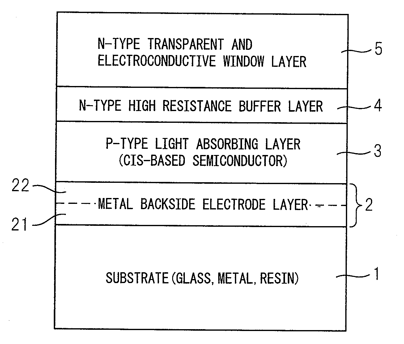
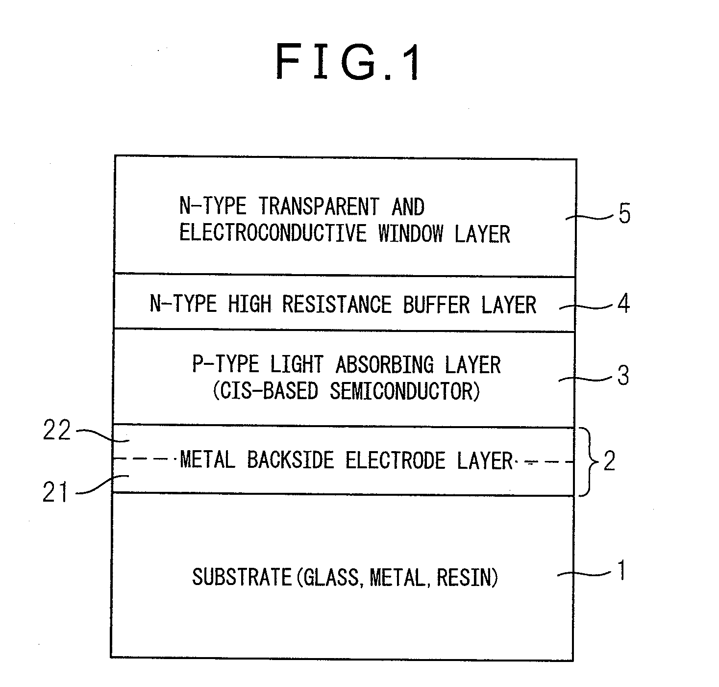
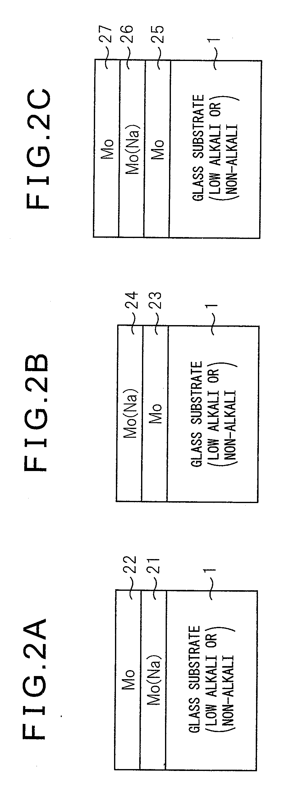
[0042]After forming a metal backside electrode on glass substrate 1 in the order of Mo layer 21 with high Na concentration and Mo layer 22 with low Na concentration, p-type light absorbing layer 3, n-type high resistance buffer layer 4 and n-type transparent and electroconductive window layer 5 were formed according to the process conditions of Table 1. On conditions that Na concentration in the low Na target was fixed to 10 at ppm and Na concentration in the high Na target was set to the four levels stated in Table 2, film thicknesses of Mo layer 21 with high Na concentration and Mo layer 22 with low Na concentration were changed. The experimental results of this case are illustrated in Table 3.

TABLE 3Experimental results 1Low NaHigh NaAverage NaHigh NafilmfilmConversionconcentrationconcentrationthicknessthicknessefficiencyin CIS[at. %][μm][μm][%][at. %]0.100.513.70.060.10.10.412.80.040.10.20.311.80.020.10.30.29.70.010.10.40.16.10.010.300.515.00.180.30.10.415.90.120.30.20.314.50.07...

experimental example 2

[0044]After forming metal backside electrode 2 in the order of Mo layer 21 with high Na concentration and Mo layer 22 with low Na concentration, p-type light absorbing layer 3, n-type high resistance buffer layer 4 and n-type transparent and electroconductive window layer 5 were formed according to the process conditions of Table 1. Then, photoelectric conversion efficiency of a resultant CIS-based thin film solar cell was measured. In this case, on conditions that Na concentration in the low Na target was set to the three levels stated in Table 2 and the Na concentration in the high Na concentration target was fixed to 1 at. %, film thicknesses of Mo layer 21 with high Na concentration and Mo layer 22 with low Na concentration were changed. The experimental results of this case are illustrated in Table 4.

TABLE 4Experimental results 2Low NaHigh NaAverage NaLow NafilmfilmConversionconcentrationconcentrationthicknessthicknessefficiencyin CIS[at. ppm][μm][μm][%][at. %]100.511.60.6810.1...


PUM


Abstract

In order to manufacture a CIS-based thin film solar cell that can achieve high photoelectric conversion efficiency by adding an alkali element to a light absorbing layer easily and with good controllability, a backside electrode layer (2) is formed on a substrate (1). Then, a p-type CIS-based light absorbing layer (3) is formed on backside electrode layer (2), and then an n-type transparent and electroconductive film (5) is formed on this p-type CIS-based light absorbing layer (3). At this time, the backside electrode layer (2) is constituted by forming a first electrode layer (21) using a backside electrode material in which an alkali metal is mixed and, then forming a second electrode layer (22) using the backside electrode material that does not substantially contain the alkali metal.

Description

FIELD[0001]The present invention relates to a method for manufacturing a CIS-based thin film solar cell, and in particular, relates to a method for manufacturing a CIS-based thin film solar cell having high photoelectric conversion efficiency and high reproducibility.BACKGROUND[0002]In recent years, a CIS-based thin film solar cell that uses a calcopyrite structure I-III-VI2 group compound semiconductor containing Cu, In, Ga, Se and S as a p-type light absorbing layer has been attracting attention. Since a solar cell of this type can be manufactured at relatively low cost and is expected to achieve high photoelectric conversion efficiency, it is widely considered a leading candidate for a next-generation solar cell. Typical materials include Cu(In, Ga)Se2, Cu(In, Ga) (Se, S)2, CuInS2, etc.[0003]In a CIS-based thin film solar cell, a metal backside electrode layer is formed on a glass substrate. A p-type light absorbing layer comprised of a I-III-VI2 group compound semiconductor is f...

Claims


Application Information

Patent Timeline
Patent Type & Authority Applications(United States)
IPC IPC(8): H01L31/032
CPCH01L31/0749Y02E10/541H01L31/03923H01L31/0323H01L31/022425Y02P70/50
Inventor HAKUMA, HIDEKITANAKA, YOSHIAKIKURIYAGAWA, SATORU
Owner SOLAR FRONTIER
Why Eureka
Try Eureka