Electromagnetic interference noise reduction board using electromagnetic bandgap structure

a technology of electromagnetic bandgap and electromagnetic interference, applied in the field of boards, can solve the problems of chronic noise problem of electromagnetic interference, more serious emi problems, and desperately needed problems to solv

Active Publication Date: 2010-08-26
SAMSUNG ELECTRO MECHANICS CO LTD
View PDF54 Cites 11 Cited by
  • Summary
  • Abstract
  • Description
  • Claims
  • Application Information

AI Technical Summary

Benefits of technology

[0009]The present invention provides an electromagnetic interference (EMI) noise reduction board that can shield the radiation noise radiated from the edge of the board by inserting an electromagnetic bandgap structure capable of shielding a noise ranging a certain frequency band into a portion of the board corresponding to the edge of the board.
[0010]The present invention also provides an EMI noise reduction board that has advantages in space utilization, production cost and power consumption, by simply modifying the structure of the board so as to easily shield the radiation noise radiated from the edge of the board.

Problems solved by technology

As the operating frequencies of electric products become higher, electromagnetic interference (EMI) has been perceived as a chronic noise problem.
Particularly, the operating frequencies of electric products have reached a few ten megahertzs (MHz), or even a few gigahertzs (GHz), making the EMI problems more serious.
Subsequently, finding a solution to the problems is desperately needed.
Among the EMI problems occurring at a board, a solution for the noise problems particularly occurred at the edge of the board has not been researched yet, making it difficult to completely shield the noise at the board.
EMI noise refers to a noise that generates a noise problem caused by an interference when an electromagnetic (EM) wave generated in one electrical circuit, component or part is transferred to another electrical circuit, component or part.

Method used


Image

  • Electromagnetic interference noise reduction board using electromagnetic bandgap structure
  • Electromagnetic interference noise reduction board using electromagnetic bandgap structure
  • Electromagnetic interference noise reduction board using electromagnetic bandgap structure

Examples


Embodiment Construction

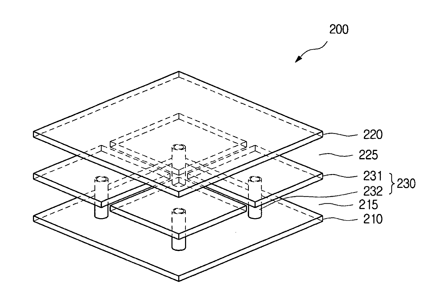
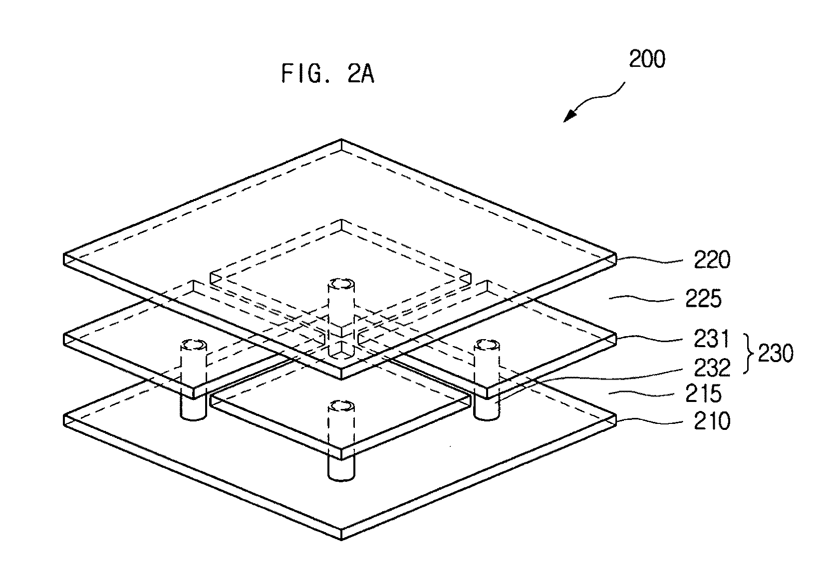
[0061]As the invention allows for various changes and numerous embodiments, particular embodiments will be illustrated in the drawings and described in detail in the written description. However, this is not intended to limit the present invention to particular modes of practice, and it is to be appreciated that all changes, equivalents, and substitutes that do not depart from the spirit and technical scope of the present invention are encompassed in the present invention.

[0062]In the description of the present invention, certain detailed descriptions of related art are omitted when it is deemed that they may unnecessarily obscure the essence of the invention.

[0063]While such terms as “first” and “second,” etc., may be used to describe various components, such components must not be limited to the above terms. The above terms are used only to distinguish one component from another. For example, a first component may be referred to as a second component without departing from the sco...


PUM


Abstract

An EMI noise reduction board using an electromagnetic bandgap structure is disclosed. In the EMI noise reduction board according to an embodiment of the present invention, an electromagnetic bandgap structure having band stop frequency properties can be inserted into an inner portion of the board so as to shield an EMI noise, in which the portion corresponds to an edge of the board and in which the EMI noise is conducted from the inside to the edge of the board and radiates to the outside of the board.

Description

CROSS-REFERENCE TO RELATED APPLICATIONS[0001]This application claims the benefit of Korean Patent Application No. 10-2009-0015332, filed with the Korean Intellectual Property Office on Feb. 24, 2009, the disclosure of which is incorporated herein by reference in its entirety.BACKGROUND[0002]1. Technical Field[0003]The present invention relates to a board, more specifically to a noise reduction board that can reduce an EMI noise by use of an electromagnetic bandgap structure.[0004]2. Description of the Related Art[0005]As the operating frequencies of electric products become higher, electromagnetic interference (EMI) has been perceived as a chronic noise problem. Particularly, the operating frequencies of electric products have reached a few ten megahertzs (MHz), or even a few gigahertzs (GHz), making the EMI problems more serious. Subsequently, finding a solution to the problems is desperately needed. Among the EMI problems occurring at a board, a solution for the noise problems par...

Claims


Application Information

Patent Timeline
Patent Type & Authority Applications(United States)
IPC IPC(8): H05K9/00
CPCH05K1/0236H05K9/002H01L2924/3025H01L2924/30107H01L2924/3011H01L2224/48227H01L2224/16225H05K9/0064H05K9/0071H05K2201/09309H05K2201/09627H01L2924/00H01L2224/0554H01L2224/05568H01L2224/05573H01L2224/16227H01L2224/16235H01L2224/48091H01L2224/48228H01L2924/00014H01L2224/05599H01L2224/0555H01L2224/0556H05K1/02H05K9/00
Inventor KIM, HANYOO, JE-GWANGRYU, CHANG-SUP
Owner SAMSUNG ELECTRO MECHANICS CO LTD
Why Eureka
Try Eureka