Semiconductor element and method for manufacturing the same

a semiconductor and light-emitting element technology, applied in the field of semiconductor elements, can solve the problems of disadvantageous degradation of the element characteristics of the semiconductor light-emitting element, and difficulty in reducing the difference between the thermal expansion coefficient of the base and the gan-based semiconductor multilayer structure as to the respective in-plane directions of the bonded surface,

Inactive Publication Date: 2010-09-02
SANYO ELECTRIC CO LTD
View PDF14 Cites 24 Cited by
  • Summary
  • Abstract
  • Description
  • Claims
  • Application Information

AI Technical Summary

Benefits of technology

[0007]As hereinabove described, the semiconductor element according to the first aspect of the present invention is provided with the semiconductor element section including the plurality of directions having the different thermal expansion coefficients in the in-plane directions of the first surface and the base including the plurality of directions having the different thermal expansion coefficients in the in-plane directions of the second surface and so formed as to bond the semiconductor element section to the base so that the direction having the largest thermal expansion coefficient in the first surface of the semiconductor element section is closer to the side of the direction having the largest thermal expansion coefficient than the direction having the smallest thermal expansion coefficient in the second surface of the base, so that the difference between the thermal expansion coefficients can be reduced in the respective in-plane directions of the plane where the first surface of the semiconductor element section and the second surface of the base are bonded to each other, whereby the first surface of the semiconductor element section can be inhibited from occurrence of strain resulting from the difference between a temperature for bonding the semiconductor element section to the base and a temperature in operation of the semiconductor element. Consequently, degradation of the element characteristics of the semiconductor element can be suppressed also when the semiconductor element section includes the plurality of directions having the different thermal expansion coefficients in the in-plane directions of the first surface.
[0027]When the largest thermal expansion coefficient and the smallest thermal expansion coefficient in the first surface of the semiconductor element section are αEL and αES respectively and the largest thermal expansion coefficient and the smallest thermal expansion coefficient in the second surface of the base are αSL and αSS respectively in the aforementioned method for manufacturing a semiconductor element according to the second aspect, the step of bonding the first surface of the semiconductor element section to the second surface of the base preferably includes a step of bonding the surfaces to each other while coinciding the directions within the second surface of the base and the first surface of the semiconductor element section with each other so that at least one relation of αSL≧αEL>αSS or αSL>αES≧αSS or αEL≧αSL>αES or αEL>αSS≧αES holds between the thermal expansion coefficients in the respective directions of the base and the semiconductor element section. According to this structure, the difference between the thermal expansion coefficients corresponding to the respective directions of the first surface of the semiconductor element section and the second surface of the base can be further reduced.

Problems solved by technology

In the semiconductor light-emitting element disclosed in Japanese Patent Laying-Open No. 2001-7394, however, the GaN-based semiconductor multilayer structure having the anisotropic thermal expansion coefficients in the in-plane directions of the principal surface is bonded to the base having the isotropic thermal expansion coefficients in the in-plane directions of the principal surface, and hence it is disadvantageously difficult to reduce the difference between the thermal expansion coefficients of the base and the GaN-based semiconductor multilayer structure as to the respective in-plane directions of the bonded surfaces.
Therefore, the GaN-based semiconductor multilayer structure is strained due to the difference between a temperature for bonding the GaN-based semiconductor multilayer structure to the base and a temperature in operation of the semiconductor light-emitting element, and hence the element characteristics of the semiconductor light-emitting element are disadvantageously degraded.

Method used


Image

  • Semiconductor element and method for manufacturing the same
  • Semiconductor element and method for manufacturing the same
  • Semiconductor element and method for manufacturing the same

Examples


first embodiment

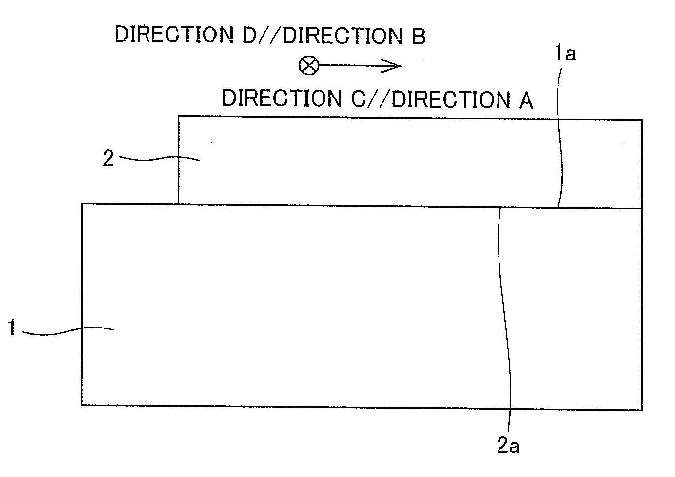
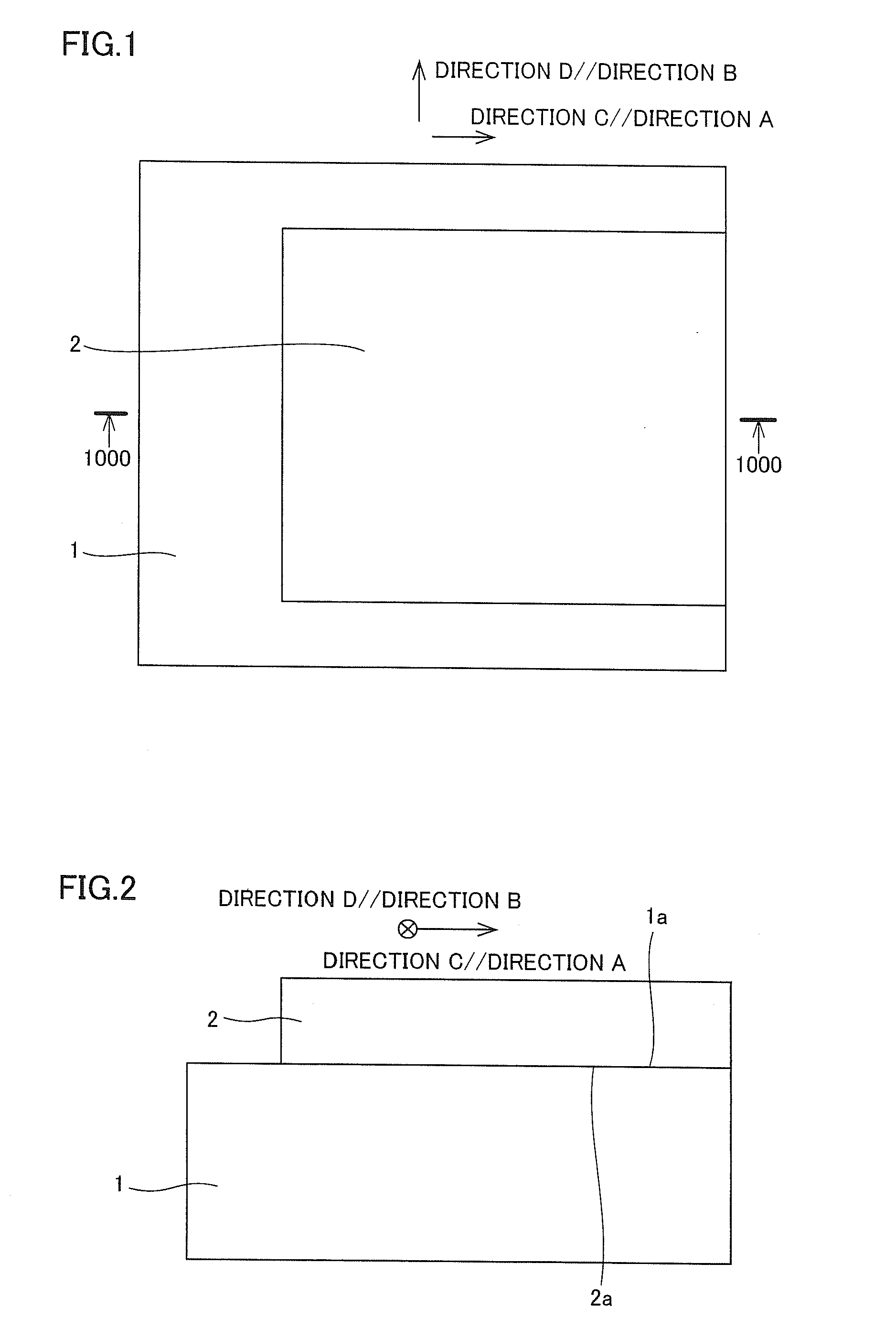
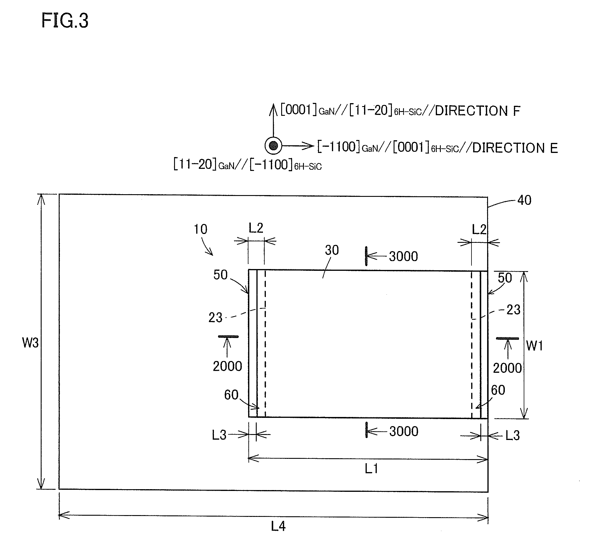
[0067]The structure of a semiconductor laser element according to a first embodiment is described with reference to FIGS. 3 to 6. The first embodiment is described with reference to a case applying the present invention to a semiconductor laser element which is an exemplary semiconductor element. The oscillation wavelength of the semiconductor laser element according to the first embodiment is about 410 nm, and a laser beam is polarized in a TM mode. Referring to FIGS. 3 to 5, crystal orientations described before a subscript GaN are the crystal orientations of a semiconductor element section 10, and crystal orientations described before a subscript 6H—SiC are the crystal orientations of a support substrate 30. FIGS. 3 and 4 show the crystal orientations of the semiconductor element section 10 omitting the misoriention angle of the semiconductor element section 10.

[0068]The semiconductor laser element according to the first embodiment comprises the semiconductor element section 10, ...

second embodiment

[0099]In this second embodiment, a GaN-based semiconductor laser element having a structure employing no support substrate dissimilarly to the aforementioned first embodiment is described with reference to FIGS. 16 and 17. The second embodiment is described with reference to the case of applying the present invention to the GaN-based semiconductor laser element which is an exemplary semiconductor element. The oscillation wavelength of the GaN-based semiconductor laser element according to the second embodiment is about 410 nm.

[0100]The GaN-based semiconductor laser element according to the second embodiment comprises a semiconductor element section 110 and a submount 140, as shown in FIGS. 16 and 17. The submount 140 is an example of the “base” in the present invention.

[0101]The semiconductor element section 110 includes an n-type GaN substrate 130 having a thickness of about 100 μm and consisting of n-type GaN doped with Si. The n-type GaN substrate 130 has a principal surface 130a...

third embodiment

[0113]The structure of an LED element according to a third embodiment is described with reference to FIGS. 18 and 19. The third embodiment is described with reference to the case of applying the present invention to the LED element which is an exemplary semiconductor element. The peak wavelength of the light-emitting diode element according to the third embodiment is about 480 nm.

[0114]The LED device according to the third embodiment comprises a support substrate 200 and an LED element section 210, as shown in FIGS. 18 and 19. The support substrate 200 is an example of the “base” in the present invention, and the LED element section 210 is an example of the “semiconductor element section” in the present invention.

[0115]The support substrate 200 has a thickness of about 300 μm, and is in the form of a square having a length of about 400 μm on each side in plan view. The support substrate 200 consists of a composite material of carbon and metal constituted of a graphite particle sinte...


PUM


Abstract

Provided is a semiconductor element which can suppress deterioration of element characteristics even when a semiconductor element section includes a plurality of directions having different thermal expansion coefficients within an in-plane direction. A semiconductor laser element (the semiconductor element) is provided with the semiconductor element section, which includes a direction of [1-100] and a direction of [0001] having different thermal expansion coefficients within the in-plane direction of a main surface, and a sub-mount, which includes an arrow (E) direction and an arrow (F) direction having different thermal expansion coefficients within the in-plane direction of the main surface. The semiconductor element section is bonded on the sub-mount so that the direction [1-100] of the semiconductor element section is close to the side of the arrow (E) direction than the arrow (F) direction of the sub-mount.

Description

TECHNICAL FIELD[0001]The present invention relates to a semiconductor element and a method for manufacturing the same, and more particularly, it relates to a semiconductor element comprising a semiconductor element section including a plurality of directions having different thermal expansion coefficients in the in-plane directions of the principal surface and a method for manufacturing the same.BACKGROUND ART[0002]In general, Japanese Patent Laying-Open No. 2001-7394 discloses a semiconductor light-emitting element (semiconductor element) comprising a GaN-based semiconductor multilayer structure (semiconductor element section) including a plurality of directions having different thermal expansion coefficients in the in-plane directions of the principal surface.[0003]In the conventional semiconductor light-emitting element disclosed in Japanese Patent Laying-Open No. 2001-7394, the GaN-based semiconductor multilayer structure having a (1-100) plane as the principal surface is formed...

Claims


Application Information

Patent Timeline
Patent Type & Authority Applications(United States)
IPC IPC(8): H01L33/02H01L21/50H01S5/022H01S5/343
CPCB82Y20/00H01S5/34333H01L33/483H01S5/0202H01S5/0224H01S5/02268H01S5/02272H01S5/02476H01S5/0425H01S5/2009H01S5/2027H01S5/22H01S5/2201H01S5/3202H01L33/16H01S2301/176H01S5/04252H01S5/04254H01S5/32025H01S5/0234H01S5/0237H01S5/02375
Inventor HATA, MASAYUKINOMURA, YASUHIKO
Owner SANYO ELECTRIC CO LTD
Why Eureka
Try Eureka