
Light emitting diode package structure

a technology of light-emitting diodes and package structures, which is applied in the direction of basic electric elements, electrical equipment, semiconductor devices, etc., can solve the problems of high manufacturing cost, difficult spot-gluing process, and inability to easily control the quantity of phosphor colloids b>11/b>/i>a /i>,

Inactive Publication Date: 2010-09-02
LEDTECH ELECTRONICS CORP
View PDF2 Cites 0 Cited by
  • Summary
  • Abstract
  • Description
  • Claims
  • Application Information

AI Technical Summary

Benefits of technology

[0009]One particular aspect of the present disclosure is to provide a light emitting diode package structure that having transparent holding walls on the surface of the substrate. A receiving space is formed in the transparent holding wall for receiving the LED. By utilizing the transparent holding wall, the colloid can be controllably received in the receiving space to uniformly cover the light emitting diode. Preferably, the distance between the LED unit and the transparent holding wall is within 5% to 10% of the width of edge of the chip. The instant disclosure therefore provides a LED structure having uniform color temperature, clear lighting, and wide light emitting angle.

Problems solved by technology

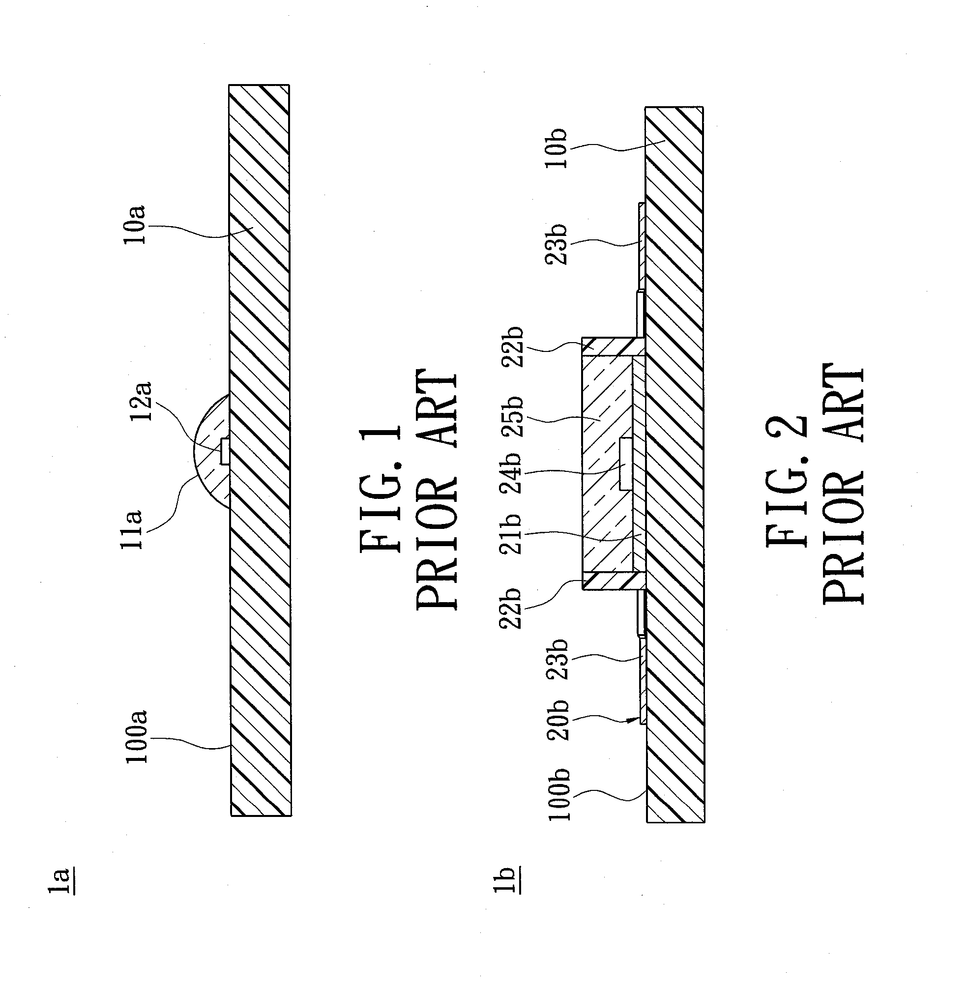
However, the spot-gluing process is difficult and the quantity of the phosphor colloid 11a can not be easily controlled.
However, the employment of a posted LED chip 20b drvies up the manufacturing cost.
Thus, the heat-dissipating efficiency is reduced.
The emission efficiency and the unit life of the LED are therefore negatively affected.

Method used


Image

  • Light emitting diode package structure
  • Light emitting diode package structure
  • Light emitting diode package structure

Examples


Embodiment Construction

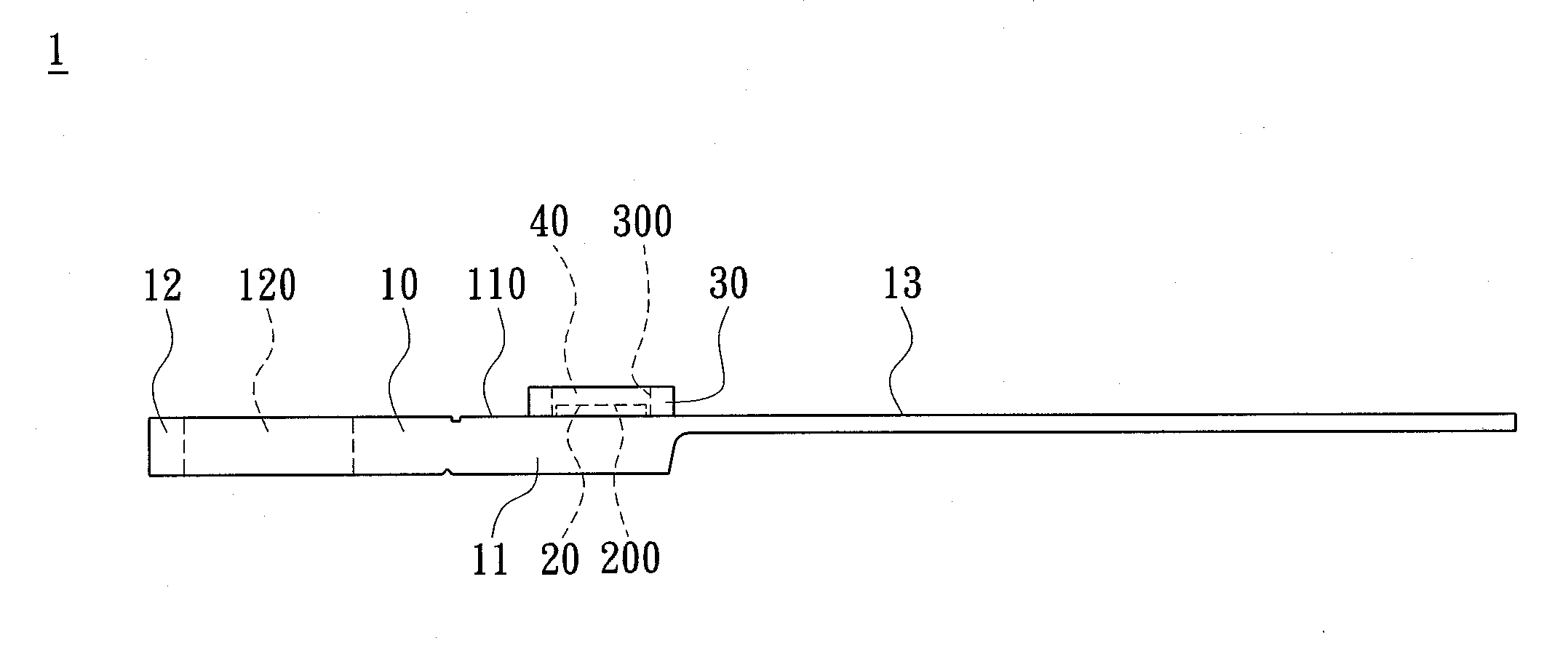
[0022]Reference is made to FIGS. 4-5, which shows a first embodiment of the present invention. The LED package structure 1 includes a substrate 10, an LED unit 20, a transparent holding wall 30, and a colloid 40. Referring to FIGS. 4A, 4B and 5. The substrate 10 can be an aluminum substrate, a copper substrate, a silver substrate, or a flexible substrate. In this particular embodiment, the substrate 10 is a LED supporting structure consisting of a copper substrate. The substrate 10 has a body portion 11, a top portion 12 and a pin portion 13. The top portion 12 and the pin portion 13 are respectively formed at the two opposing ends of the body portion 11. The body portion 11 has a package surface 110 for receiving the LED unit 20 and the colloid 40. The top portion 12 has a positioning hole 120 for positioning the package. The pin portion 13 is used for connecting with an external electronic device (not shown in the figure) to establish electrical connection. The LED unit 20 is elec...


PUM


Abstract

An LED package structure and an LED packaging method are disclosed. The LED package structure includes a substrate, an LED unit and a transparent holding wall. The LED unit is electrically connected and located on the surface of the substrate. The transparent holding wall that corresponds to the LED unit is formed on the surface of the substrate, and has a receiving space. The LED unit is received in the receiving space. By utilizing the transparent holding wall, the colloid is controllably received in the receiving space and uniformly spread on the surface of the LED unit and around the LED unit. Thereby, the quantity of the colloid is easily controlled, and the LED package structure has a wide lighting angle due to the light emitted from the LED unit can pass through the transparent holding wall.

Description

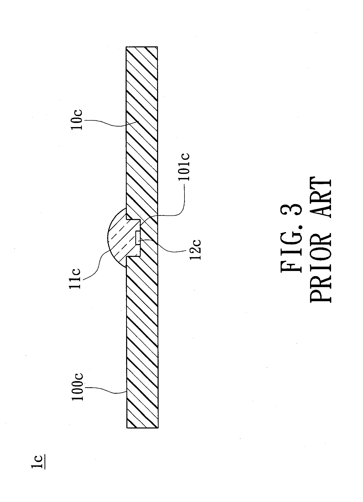
CROSS REFERENCE TO RELATED APPLICATION[0001]This application is a continuation-in-part of U.S. application Ser. NO. 12 / 071842, filed on Feb. 27, 2008, now pending.BACKGROUND OF THE INVENTION[0002]1. Field of the Invention[0003]The present invention relates to a package structure. In particular, the invention relates to a light emitting diode package structure for receiving the colloid so that the colloid is controllable and is uniformly covered the light emitting diode.[0004]2. Description of the Related Art[0005]Reference is made to FIG. 1, which shows a schematic diagram of the light emitting diode (LED) package structure of the prior art. The LED package structure la includes a substrate 10a, a phosphor colloid 11a, and an LED 12a. The phosphor colloid 11a and the LED 12a are respectively located on the package surface 100a of the substrate 10a. In the prior art, the phosphor colloid 11a is packaged on the LED 12a by a spot-gluing method to achieve the lighting effect of the LED....

Claims


Application Information

Patent Timeline
Patent Type & Authority Applications(United States)
IPC IPC(8): H01L33/00
CPCH01L25/0753H01L33/54H01L33/505H01L33/483H01L2924/0002H01L2924/00
Inventor KUO, JUI-LUNWANG, YAO-IWANG, FANG-PO
Owner LEDTECH ELECTRONICS CORP
Learn More