Method of multi-element compound deposition by atomic layer deposition for IC barrier layer applications

a technology of ic barrier layer and compound, which is applied in the direction of single crystal growth, polycrystalline material growth, chemistry apparatus and processes, etc., can solve the problems of reducing device performance, poor coverage of certain parts of the via opening, and difficult conventional chemical vapor deposition method of forming a uniform diffusion barrier layer, etc., to achieve good cu barrier capability, improve the performance of the mosfet transistor, and uniform step coverage

Inactive Publication Date: 2005-03-03
TAIWAN SEMICON MFG CO LTD
View PDF11 Cites 33 Cited by
  • Summary
  • Abstract
  • Description
  • Claims
  • Application Information

AI Technical Summary

Benefits of technology

[0014] A further objective of the present invention is to provide an ALD method for fabricating a gate dielectric layer with improved performance in a MOSFET transistor.
[0015] A still further objective ...

Problems solved by technology

When the trench or via opening becomes smaller and a thinner diffusion barrier layer is required, a conventional chemical vapor deposition (CVD) method of forming a uniform diffusion barrier layer becomes very difficult.
This nonuniformity can lead to poor coverage of certain parts of a via opening such as bottom corners, for example.
As a result, when copper is deposited, small voids can form between the metal layer and via sidewall that will detract from device performance.
In other cases, insufficient barrier layer coverage in certain regions of a via or trench will not protect Cu from moisture or traces of other corrosive agents ...

Method used


Image

  • Method of multi-element compound deposition by atomic layer deposition for IC barrier layer applications
  • Method of multi-element compound deposition by atomic layer deposition for IC barrier layer applications
  • Method of multi-element compound deposition by atomic layer deposition for IC barrier layer applications

Examples


first embodiment

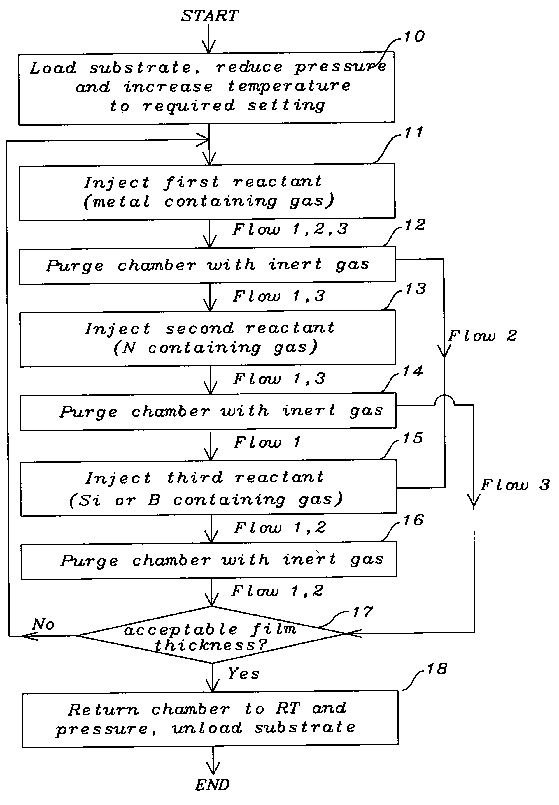
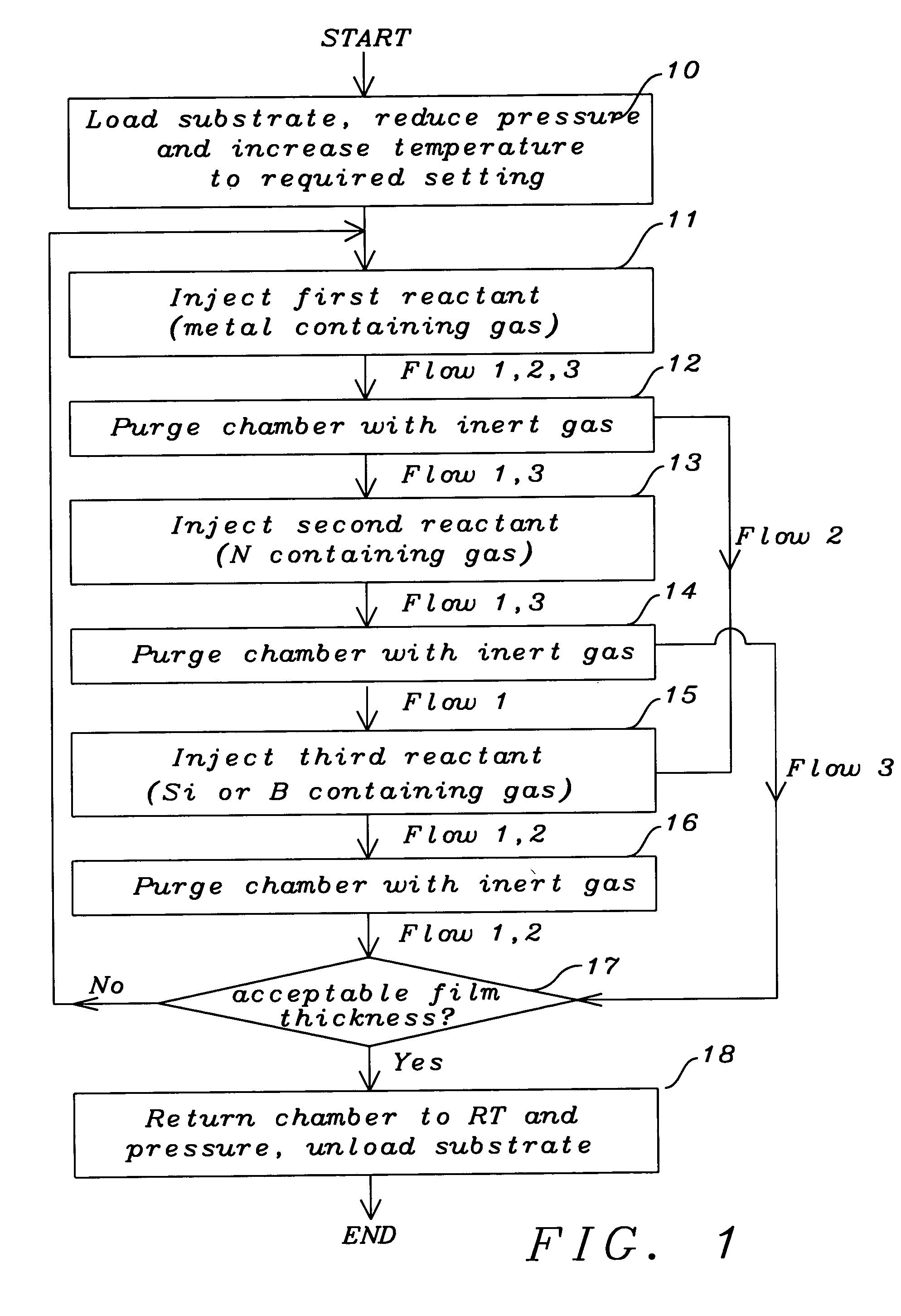
[0037] In a first embodiment, a composite layer comprised of three elements is applied with an ALD method and is especially useful as a diffusion barrier layer for Cu in an interconnect structure. However, the ALD deposited layer is not limited to barrier layer applications or to interconnect structures and may be used wherever a composite layer containing three elements is employed in a semiconductor device. The composite layer has the formula M1VSXNZ where M1 is a metal, S is Si or B, and N is nitrogen and where V, X, and Z are fractions between 0 and 1 that together equal 1.

[0038] Referring to FIG. 1, a flow diagram shows a representative method for an ALD sequence comprised of a plurality of cycles that each form a monolayer and collectively form a composite layer. A substrate is provided and is loaded into a process chamber in an ALD tool in step 10. Typically, the substrate is secured to a chuck or pedestal in the process chamber. The ALD process tool may be an Endura system ...

second embodiment

[0056] In a second embodiment, a composite metal oxide layer comprised of three elements is applied with an ALD method and serves as a high k dielectric layer in a MOSFET device that may be a n-type (NMOS) or p-type (PMOS) transistor. The composite layer has the formula. M1PM2QOR where M1 is a first metal, M2 is a second metal, O is oxygen and where P, Q, and R are fractions between 0 and 1 that when added together equal 1.

[0057] Referring to FIG. 3, a flow diagram shows a representative method for an ALD sequence that provides a composite metal oxide layer. A substrate is provided and is loaded into a process chamber in an ALD tool in step 30. Typically, the substrate is secured to a chuck or pedestal in the process chamber which is part of an ALD tool described in the first embodiment. Step 30 also involves heating the chamber so that the substrate reaches a temperature in the range of 100° C. to 500° C. which is maintained until the ALD process is completed. Additionally, all ga...

third embodiment

[0069] In a third embodiment, a composite layer comprised of four elements is formed by an ALD method. In one aspect, the composite layer serves as a diffusion barrier layer in a Cu interconnect scheme. However, the ALD deposited layer is not limited to barrier layer applications or to interconnect structures and may be employed in any semiconductor device where a composite layer containing four elements is useful. The composite layer has the formula M1vM2WSXNZ where M1 is a first metal, M2 is a second metal, S is Si or B, and N is nitrogen and where V, W, X, and Z are fractions between 0 and 1 and which added together equal 1.

[0070] Referring to FIG. 5, a flow diagram shows a method including a cycle F and a cycle G that may be performed in various orders in an ALD sequence to deposit a composite layer comprised of four elements. A substrate is loaded into a process chamber in an ALD tool in step 50 and the chamber is prepared for processing as described in step 30.

[0071] Beginni...


PUM


Abstract

An ALD method is described for depositing a composite layer comprised of three to five elements including one or two metals, Si, B and N. A metal containing gas is injected into a process chamber and purged followed by a N source gas and a purge and/or a Si or B source gas and a purge to complete a cycle and form a monolayer. A predetermined number of monolayers each having two or three elements is deposited to provide a composite film with good step coverage and a well controlled composition. The resulting layer is especially useful as a diffusion barrier layer for copper. Alternatively, a three component layer comprised of Hf, Zr, and O may be deposited and serves as a gate dielectric layer in a MOSFET device. The invention is also a thin film comprised of a plurality of monolayers each having two or three elements.

Description

RELATED PATENT APPLICATION [0001] This application is related to the following: Docket # TSMC01-1247, Ser. No. ______, filing date ______, assigned to a common assignee.FIELD OF THE INVENTION [0002] The invention relates to the field of fabricating integrated circuits and in particular to an atomic layer deposition (ALD) method of forming a multi-element film that is used as a diffusion barrier layer or as a gate dielectric layer during the fabrication of a semiconductor device. BACKGROUND OF THE INVENTION [0003] As the gate length of polysilicon gates in transistor devices and the width of wiring in metal interconnects continues to shrink in semiconductor manufacturing, the thickness of layers used to protect and insulate these conductive features is also decreasing. For example, metal interconnects for new technologies that have a critical dimension (CD) approaching 100 nm are fabricated with copper and are protected by a thin diffusion barrier layer that is conformally deposited ...

Claims


Application Information

Patent Timeline
IPC IPC(8): C30B25/02C30B25/14H01L21/314H01L21/316
CPCC30B25/02C30B25/14H01L21/31645H01L21/31641H01L21/3141H01L21/02189H01L21/02181H01L21/0228
Inventor WU, CHII-MINGPENG, CHAO-HSIENSHUE, SHAU-LIN
Owner TAIWAN SEMICON MFG CO LTD
Why Eureka
Try Eureka