Two-Sided Semiconductor Structure

a semiconductor structure and semiconductor technology, applied in the field of semiconductor structures, can solve the problems of high cost of tools and the same cost of an initial (unprocessed) substrate per semiconductor device, and achieve the effect of reducing the cost of semiconductor devices and reducing the cost of tools

Active Publication Date: 2010-09-09
IBM CORP
View PDF2 Cites 257 Cited by
  • Summary
  • Abstract
  • Description
  • Claims
  • Application Information

AI Technical Summary

Problems solved by technology

While it is possible to reduce the overlay tolerance by employing accurate alignment tools, such tools are typically costly.
Thus, the cost of an initial (unprocessed) substrate per semiconductor device is the same between three-dimensionally stacked semiconductor chips and a non-stacked semiconductor chip.

Method used


Image

  • Two-Sided Semiconductor Structure
  • Two-Sided Semiconductor Structure
  • Two-Sided Semiconductor Structure

Examples


Embodiment Construction

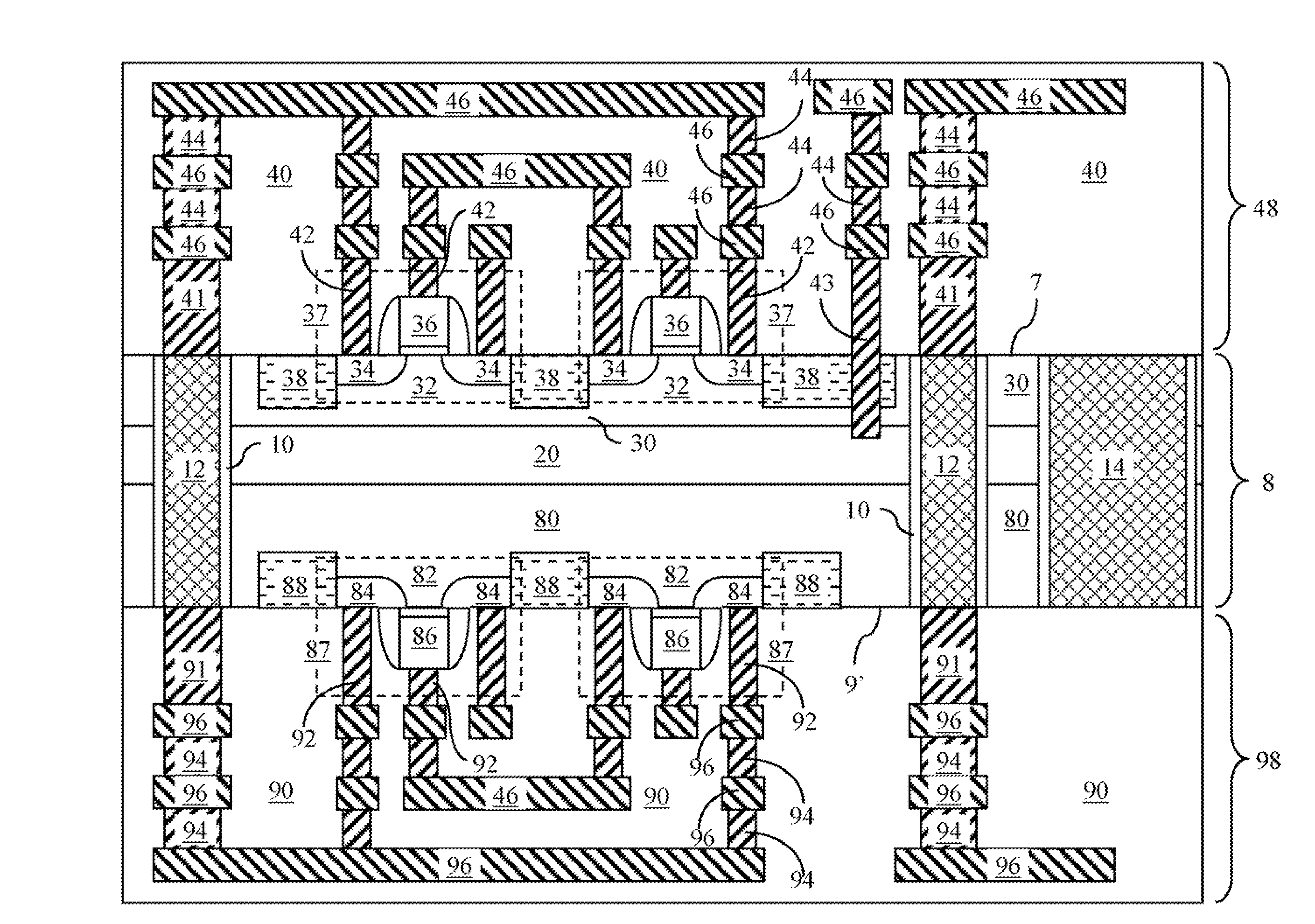
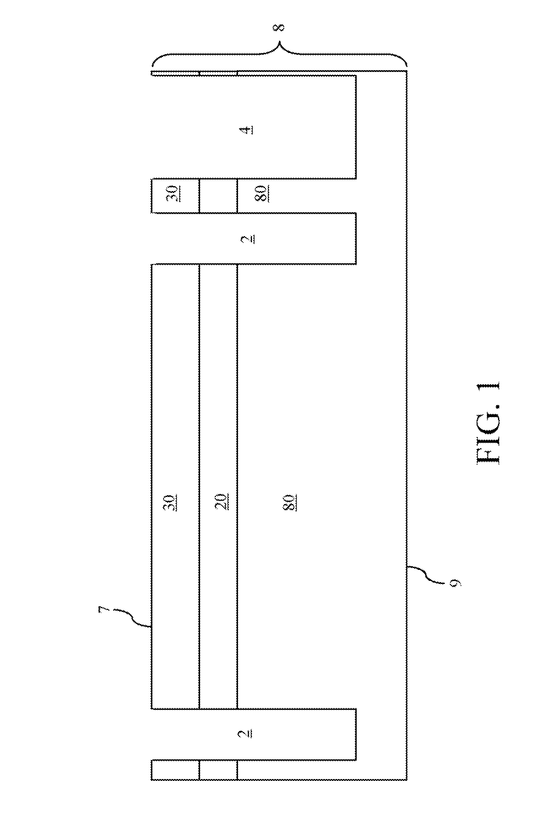
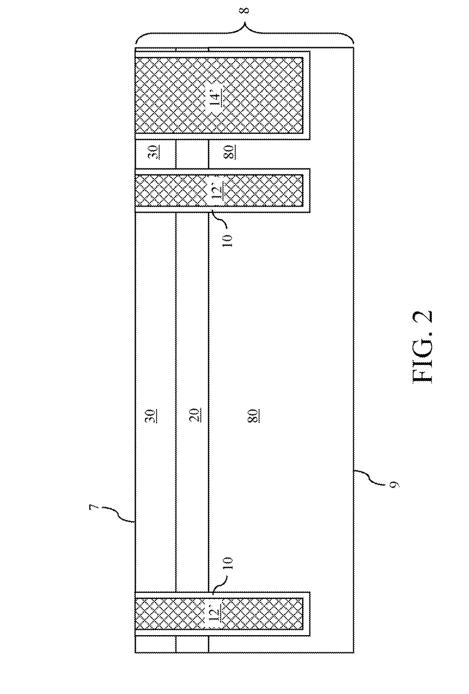
[0021]As stated above, the present invention relates to semiconductor structures including semiconductor devices on opposing pair of surfaces, i.e., both sides, of a semiconductor substrate and methods of manufacturing the same, which is now described in detail with accompanying figures. Like and corresponding elements are referred to by like reference numerals.

[0022]Referring to FIG. 1, a buried conductive layer 20 is formed in a semiconductor substrate 8. The semiconductor substrate 8 is a bulk substrate including a semiconductor material. The semiconductor material may be selected from, but is not limited to, silicon, germanium, silicon-germanium alloy, silicon carbon alloy, silicon-germanium-carbon alloy, gallium arsenide, indium arsenide, indium phosphide, III-V compound semiconductor materials, II-VI compound semiconductor materials, organic semiconductor materials, and other compound semiconductor materials. Preferably, the entirety of the semiconductor material within the se...


PUM


Abstract

Deep via trenches and deep marker trenches are formed in a bulk substrate and filled with a conductive material to form deep conductive vias and deep marker vias. At least one first semiconductor device is formed on the first surface of the bulk substrate. A disposable dielectric capping layer and a disposable material layer are formed over the first surface of the bulk substrate. The second surface, located on the opposite side of the first surface, of the bulk substrate is polished to expose and planarize the deep conductive vias and deep marker vias, which become through-substrate vias and through-substrate alignment markers, respectively. At least one second semiconductor device and second metal interconnect structures are formed on the second surface of the bulk substrate. The disposable material layer and the disposable dielectric capping layer are removed and first metal interconnect structures are formed on the first surface.

Description

[0001]This non-provisional application claims the benefit of the provisional application filed with the U.S. Patent and Trademark Office as Ser. No. 61 / 157,638 entitled “Two-Sided Semiconductor Structure”, filed Mar. 5, 2009.FIELD OF THE INVENTION[0002]The present invention relates to semiconductor structures including semiconductor devices on both sides of a semiconductor substrate and methods of manufacturing the same.BACKGROUND OF THE INVENTION[0003]Three-dimensional integration of semiconductor chips typically employs through-substrate vias (TSV's) that connect the front side of a semiconductor chip to a back side of the same semiconductor chip. Multiple semiconductor chips may be vertically stacked employing the through-substrate vias (TSV's). Such three-dimensional integration of semiconductor chips provides a higher device density per area than a single semiconductor chip without any vertical stacking, and reduces the size of a packaging substrate correspondingly.[0004]While ...

Claims


Application Information

Patent Timeline
Patent Type & Authority Applications(United States)
IPC IPC(8): H01L29/04H01L23/48H01L21/768
CPCH01L21/743H01L21/76898H01L2924/0002H01L21/8221H01L23/481H01L23/544H01L27/0694H01L2223/5442H01L2223/54426H01L2223/5448H01L2924/12044H01L2924/19041H01L2924/19042H01L2924/19043H01L2924/00
Inventor ZHU, HUILONG
Owner IBM CORP
Why Eureka
Try Eureka