
Configurable logic integrated circuit having a multidimensional structure of configurable elements

a technology of configurable elements and integrated circuits, which is applied in the direction of memory address/allocation/relocation, instruments, and architectures with multiple processing units, etc., can solve the problems that synthesis tools cannot map these loops onto hardware, recursions basically cannot be mapped onto hardware, and hardware has to be made availabl

Inactive Publication Date: 2010-09-09
SCIENTIA SOL MENTIS AG
View PDF106 Cites 19 Cited by
  • Summary
  • Abstract
  • Description
  • Claims
  • Application Information

AI Technical Summary

Benefits of technology

[0007]An object of the present invention is to provide a programming method which allows the above-described hardware modules to be efficiently programmed with conventional high-level programming languages, making automatic, full, and efficient use of the parallelism of the above-described hardware modules obtained by the plurality of units to the maximum possible degree.

Problems solved by technology

1. A programmer must become accustomed to programming in data flow languages; multilevel sequential tasks can generally be described only in a complex manner;
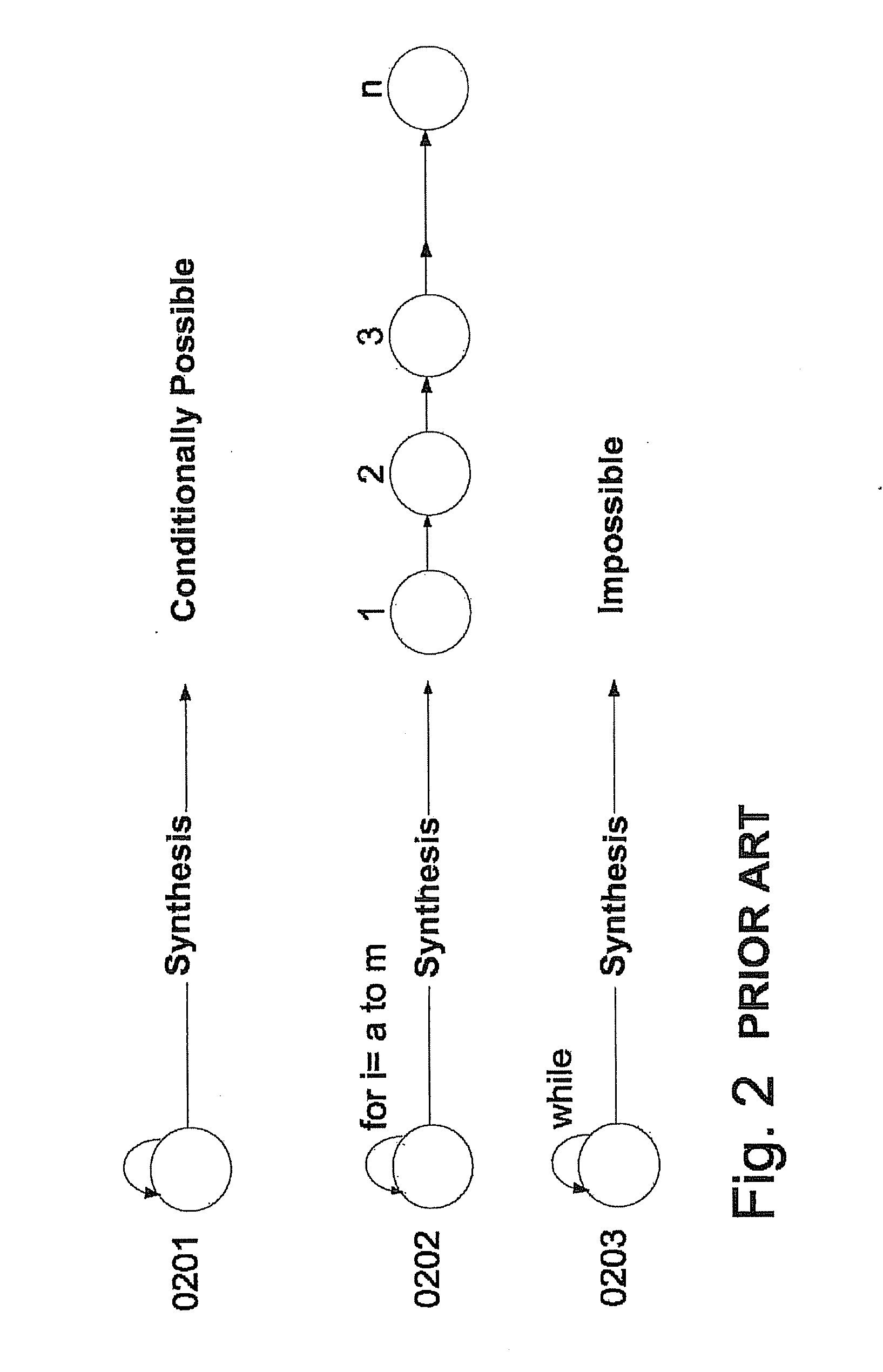
2. Large applications and sequential descriptions can be mapped to the desired target technology (synthesized) with the existing translation programs (synthesis tools) only to a certain extent.
Due to their dynamic behavior, these synthesis tools cannot map these loops onto the hardware, e.g., transfer them to a target module, in a fixed manner.
Using conventional synthesis tools, recursions basically cannot be mapped onto hardware if the recursion depth is not known at the time of the synthesis.
This would mean that new hardware has to be made available with each recursion level, which, however, is dynamically impossible.

Method used


Image

  • Configurable logic integrated circuit having a multidimensional structure of configurable elements
  • Configurable logic integrated circuit having a multidimensional structure of configurable elements
  • Configurable logic integrated circuit having a multidimensional structure of configurable elements

Examples


example stack

Model

[0125]A simple stack processor may be designed by using the REQ / ACK protocol and the internal memory in the LIFO mode. In this mode, temporary data is written by the PAEs to the stack and loaded from the stack as needed. The necessary compiler technologies are sufficiently known. The stack may be as large as needed due to the variable stack depth, which is achieved through a data exchange of the internal memory with an external memory.

Example Accumulator Model

[0126]Each PAE can represent an arithmetic unit according to the accumulator principle. As described in German Patent Application No. 196 51 075.9, the output register may be looped back to the input of the PAE. This yields structure which may operate like a related art accumulator. Simple accumulator processors can be designed in connection with the sequencer according to FIG. 11.

example register

Model

[0127]A simple register processor can be designed by using the REQ / ACK protocol and the internal memory in the standard memory mode. The register addresses are generated by one group of PAEs, while another group of PAEs is responsible for processing the data.

Example Memory Architecture

[0128]The example memory has two interfaces: a first interface which connects the memory to the array, and a second one which connects the memory with an IO unit. In order to improve the access time, the memory may be designed as a dual-ported RAM, which allows read and write accesses to take place independently of one another.

[0129]The first interface may be a conventional PAE interface (PAEI), which may guarantee access to the bus system of the array and may ensure synchronization and trigger processing. Triggers can be used to display different states of the memory or to force actions in the memory, for example,

1. Empty / full: when used as a FIFO, the FIFO status “full,”“almost full,”“empty,” or...

example compiler

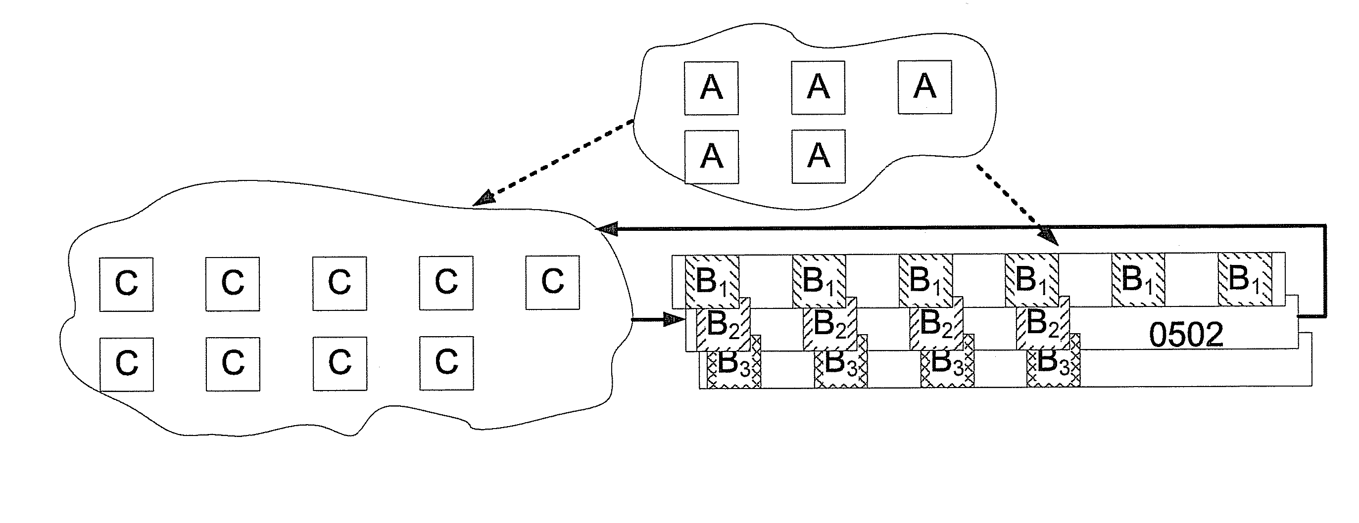
[0149]In an example embodiment according to the present invention, the VPU technology programming may include separating sequential codes and breaking them down into the largest possible number of small and independent subalgorithms, while the subalgorithms of the data flow code may be mapped directly onto the VPU.

Separation Between VPU Code and Standard Code

[0150]C++ is used in the following to represent all possible compilers (Pascal, Java, Fortran, etc.) within a related art language; a special extension (VC=VPU C), which contains the language constructs and types which can be mapped onto VPU technology particularly well, may be defined. VC may be used by programmers only within methods or functions that use no other constructs or types. These methods and functions can be mapped directly onto the VPU and run particularly efficiently. The compiler extracts the VC in the pre-processor and forwards it directly to the VC back-end processing (VCBP).

[0151]Extraction of the parallelizab...


PUM


Abstract

Programming of modules which can be reprogrammed during operation is described. Partitioning of code sequences is also described.

Description

AREA OF APPLICATION[0001]The present invention may be applied to programmable arithmetic and / or logic hardware modules (VPUs) which can be reprogrammed during operation. For example, the present invention may be applied to VPUS having a plurality of arithmetic and / or logic units whose interconnection can also be programmed and reprogrammed during operation. Such logical hardware modules are available from several manufacturers under the generic name of FPGA (Field-Programmable Gate Arrays). Furthermore, several patents have been published, which describe special arithmetic hardware modules having automatic data synchronization and improved arithmetic data processing.[0002]All the above-described hardware modules may have a two-dimensional or multidimensional arrangement of logical and / or arithmetic units (Processing Array Elements—PAEs) which can be interconnected via bus systems.[0003]The above described hardware modules may either have the units listed below or these units may be ...

Claims


Application Information

Patent Timeline
IPC IPC(8): G06F15/80G06F9/06G06F12/00G06F12/08G06F11/00G06F9/45
CPCG06F8/433G06F15/7867G06F15/80G06F8/45
Inventor VORBACH, MARTINNUCKEL, ARMIN
Owner SCIENTIA SOL MENTIS AG
Learn More