Gated diode having at least one lightly-doped drain (LDD) implant blocked and circuits and methods employing same

a gated diode and drain technology, applied in the field of gated diodes, can solve the problems of affecting the performance of the protected circuit, the inability to use gated diodes in the esd protection circuit, etc., and achieve the effects of enhanced esd protection circuit, fast turn-on times, and high conductance characteristics of the gated diod

Inactive Publication Date: 2010-09-16
QUALCOMM INC
View PDF23 Cites 35 Cited by
  • Summary
  • Abstract
  • Description
  • Claims
  • Application Information

AI Technical Summary

Benefits of technology

[0013]The gated diode having at least one blocked LDD implant can be included in any circuit, integrated circuit, or circuit application. One example includes an electro-static discharge (ESD) protection circuit. An ESD protection circuit is enhanced by fast turn-on times and high conductance characteristics of the gated diode. However, if the ESD protection circuit employs one or more of the gated diodes having at least one LDD implant blocked, the capacitance of the ESD protection circuit is reduced as well. This may allow the ESD protection circuit to be employed to protect circuits whose performance is sensitive to load capacitance while still achieving the ESD characteristics of gated diodes. Otherwise, use of gated diodes in the ESD protection circuit may not be possible without affecting the protected circuit's performance in an unacceptable manner. Other examples of protected circuits whose performance may be sensitive to load capacitance and thus may benefit from the gated diodes disclosed herein include high speed differential input / output circuits and radio frequency (RF) circuits, including but not limited to low noise amplifiers (LNAs).

Problems solved by technology

Otherwise, use of gated diodes in the ESD protection circuit may not be possible without affecting the protected circuit's performance in an unacceptable manner.

Method used


Image

  • Gated diode having at least one lightly-doped drain (LDD) implant blocked and circuits and methods employing same
  • Gated diode having at least one lightly-doped drain (LDD) implant blocked and circuits and methods employing same
  • Gated diode having at least one lightly-doped drain (LDD) implant blocked and circuits and methods employing same

Examples


Embodiment Construction

[0024]With reference now to the drawing figures, several exemplary embodiments of the present disclosure are described. The word “exemplary” is used herein to mean “serving as an example, instance, or illustration.” Any embodiment described herein as “exemplary” is not necessarily to be construed as preferred or advantageous over other embodiments.

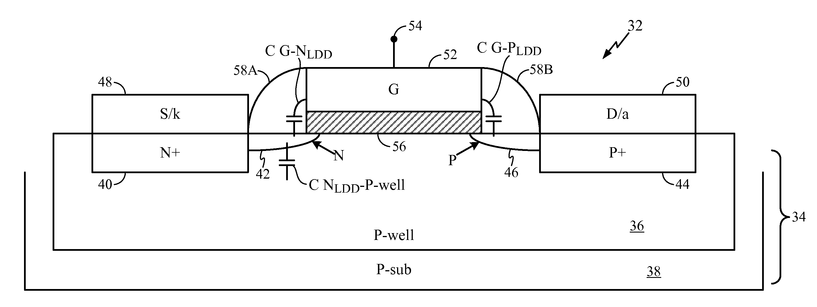
[0025]Embodiments disclosed in the detailed description include examples of gated diodes, exemplary methods of manufacture of the same, and related circuits and methods. The gated diode examples all have at least one lightly-doped drain (LDD) implant blocked to reduce capacitance of the gated diode. In this manner, the gated diode may be employed in circuits and other circuit applications whose performance may be sensitive to load capacitance, but also desire or require the performance characteristics of a gated diode. Benefits of a gated diode include, but are not limited to, fast turn-on times and high conductance.

[0026]In embodiments di...


PUM


Abstract

Gated diodes, manufacturing methods, and related circuits are provided wherein at least one lightly-doped drain (LDD) implant is blocked in the gated diode to reduce its capacitance. In this manner, the gated diode may be used in circuits and other applications whose performance is sensitive to load capacitance while still obtaining the performance characteristics of a gated diode. These characteristics include fast turn-on times and high conductance, making the gated diodes disclosed herein well-suited for electro-static discharge (ESD) protection circuits as one application example. The examples of the gated diode disclosed herein include a semiconductor substrate having a well region and insulating layer thereupon. A gate electrode is formed over the insulating layer. Anode and cathode regions are provided in the well region, wherein a P-N junction is formed. At least one LDD implant is blocked in the gated diode to reduce capacitance.

Description

BACKGROUND[0001]I. Field of the Disclosure[0002]The technology of the present application relates to gated diodes and their use in circuits and related methods, including protection circuits, electro-static discharge (ESD) protection circuits, and high speed or switching circuits.[0003]II. Background[0004]Electro-static discharge (ESD) is a major reliability issue in integrated circuits (ICs). ESD is a transient surge in voltage (negative or positive) that may induce a large current in a circuit. To protect circuits against damage from ESD surges, protection schemes attempt to provide a discharge path for both positive and negative ESD surges. Conventional diodes can be employed in ESD protection circuits to clamp the voltage of positive and negative ESD surges to shunt current and prevent excessive voltage from being applied to a protected circuit. FIG. 1 illustrates a conventional ESD protection circuit in this regard. As illustrated in FIG. 1, a voltage rail (Vdd) 10 and a ground...

Claims


Application Information

Patent Timeline
Patent Type & Authority Applications(United States)
IPC IPC(8): H02H9/04H01L21/336H01L29/78
CPCH01L27/0255H01L29/66356H01L29/7391H04B1/48H01L2924/0002H01L2924/00
Inventor WORLEY, EUGENE R.
Owner QUALCOMM INC
Why Eureka
Try Eureka