
Method of manufacturing silicon carbide seminconductor device

Active Publication Date: 2010-09-16
DENSO CORP
View PDF2 Cites 0 Cited by
  • Summary
  • Abstract
  • Description
  • Claims
  • Application Information

AI Technical Summary

Benefits of technology

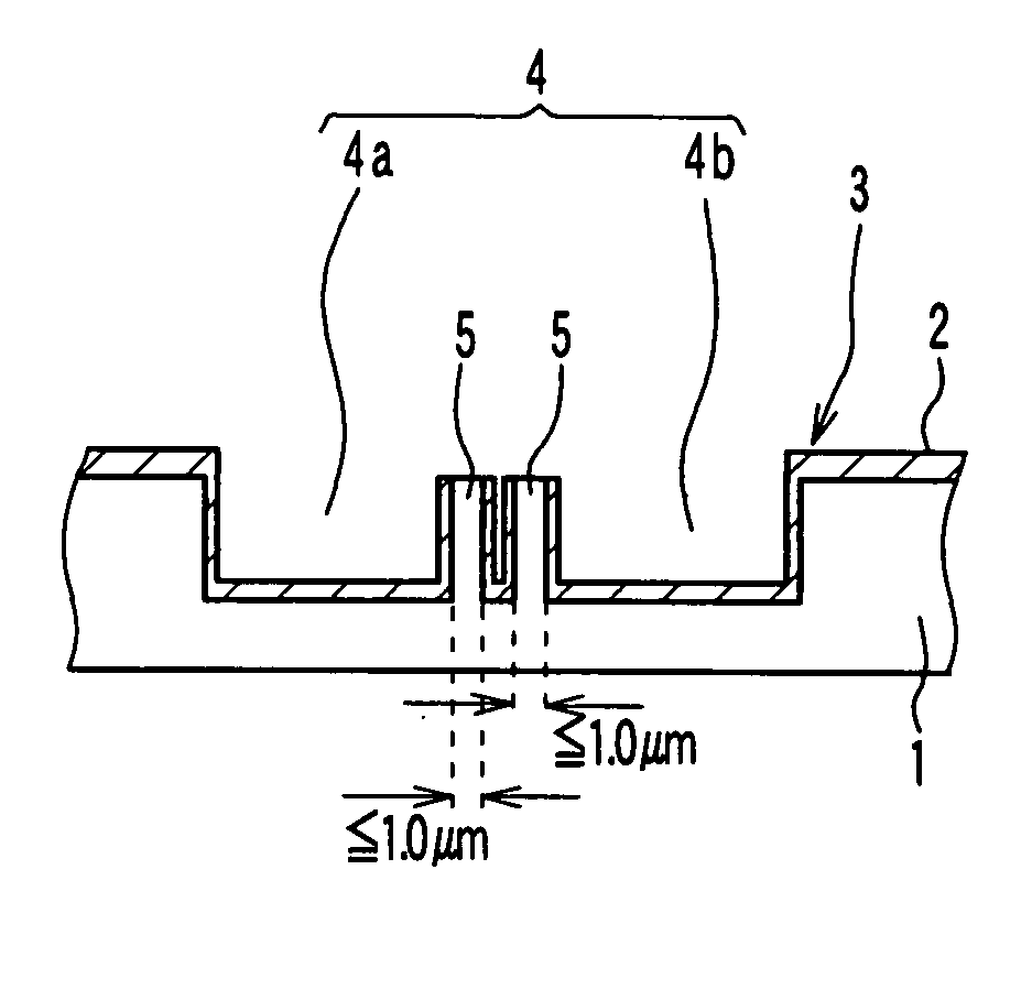
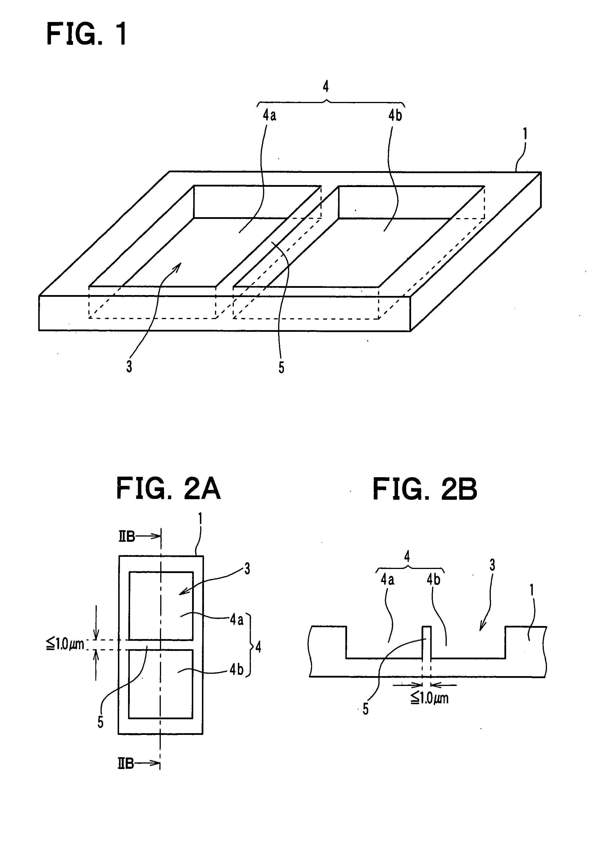
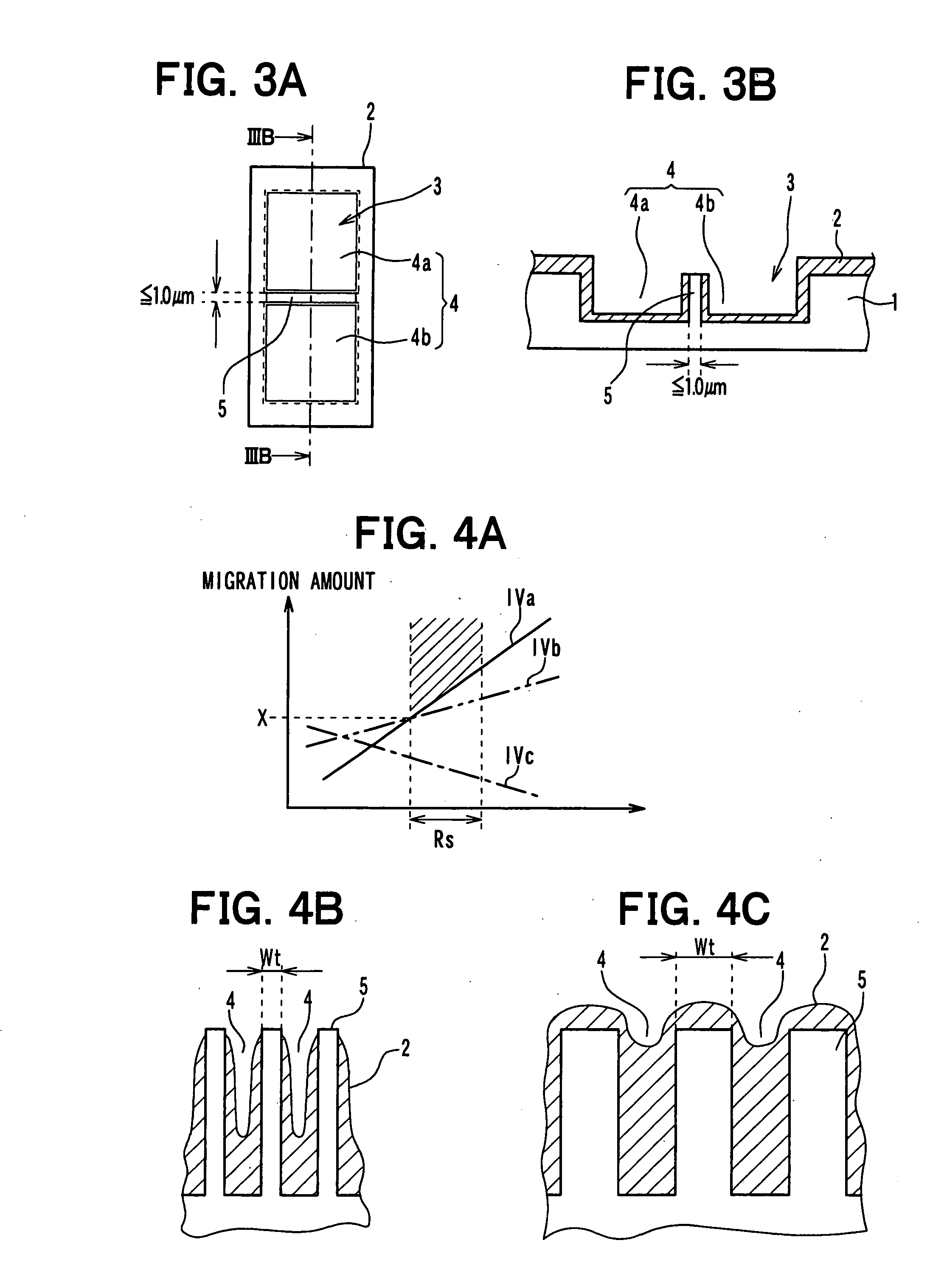
[0013]In a method of manufacturing a silicon carbide semiconductor device according to an aspect of the present invention, a trench and a thickness measurement section are formed in a surface of a semiconductor substrate made of silicon carbide. The thickness measurement section includes a plurality of grooves and a protruding portion. The protruding portion is provided between the grooves so as to extend in one direction and have a predetermined width. An epitaxial layer made of silicon carbide is grown on the surface of the semiconductor substrate, a bottom surface and a sidewall of the trench, and a bottom surface and a sidewall of the plurality of grooves. During growth of the epitaxial layer, a thickness of the epitaxial layer formed on the surface of the semiconductor substrate is measured by calculating a difference in height between a surface of the epitaxial layer formed on a portion of the surface of the semiconductor substrate different from the thickness measurement section and a top su

Problems solved by technology

When the epitaxial layer is formed in the trenches by the conventional technique, it is difficult to form the epitaxial layer only on the sidewalls as the channel forming planes, and the epitaxial layer grows on a surface of the substrate, the sidewalls of the trenches, and bottom surfaces of the trenches along shapes of the trenches.
Therefore, it is difficult to control the thickness of the epitaxial layer appropriately unless the epitaxial layer is observed in a manufacturing process.

Method used


Image

  • Method of manufacturing silicon carbide seminconductor device
  • Method of manufacturing silicon carbide seminconductor device
  • Method of manufacturing silicon carbide seminconductor device

Examples


first embodiment

[0033]A manufacturing method of an SiC semiconductor device according to a first embodiment of the present invention will now be described. The manufacturing method according to the present embodiment can be used, for example, for forming an SiC semiconductor device including an accumulation MOSFET having a trench gate structure. A structure of the accumulation MOSFET is similar to a conventional accumulation MOSFET described, for example, in U.S. Pat. No. 5,744,826. A method of forming an N type epitaxial layer in the accumulation channel and a method of measuring a thickness of the N type epitaxial layer will be described with reference to FIG. 1 to FIG. 5C.

[0034]Before forming an N type epitaxial layer 2 on a semiconductor substrate 1 made of SiC as shown in FIG. 3, a thickness measurement section 3 shown in FIG. 1, FIG. 2A and FIG. 2B is formed.

[0035]The thickness measurement section 3 is formed at a region of the semiconductor substrate 1 other than a chip forming region where ...

second embodiment

[0052]A manufacturing method of an SiC semiconductor device according to a second embodiment of the present invention will now be described. In the method according to the present embodiment, a thickness measurement section 3 is formed in the semiconductor substrate 1 as shown FIG. 6A to FIG. 6C.

[0053]The thickness measurement section 3 according to the present embodiment includes a plurality of protruding portions 5 (in the example shown in FIG. 6A to FIG. 6C, two protruding portions 5) between the first groove 4a and the second groove 4b. The protruding portions 5 are parallel to each other. A width Wt of each of the protruding portions 5 is set to be, for example, less than 1.0 μm, in a manner similar to the first embodiment. A distance between the protruding portions 5 is set to be more than two times a predetermined thickness of the N type epitaxial layer 2 that is formed in a later process so that a portion between the protruding portions 5 is not fully filled with the N type ...

third embodiment

[0056]A manufacturing method of an SiC semiconductor device according to a third embodiment of the present invention will now be described.

[0057]In the method according to the present embodiment, a first thickness measurement section 3a and a second thickness measurement section 3b are formed in the semiconductor substrate 1 as shown in FIG. 7. In FIG. 7, the first thickness measurement section 3a, the second thickness measurement section 3b, and a trench 10 for forming a trench gate of an accumulation MOSFET are magnified.

[0058]In a case where the trench 10 for forming the trench gate of the accumulation MOSFET extends in one direction on a surface of a semiconductor substrate 1, the first thickness measurement section 3a is formed in such a manner that a protruding portion 5 of the first thickness measurement section 3a extends in a direction parallel to the one direction, and the second thickness measurement section 3b is formed in such a manner that a protruding portion 5 of the...


PUM


Abstract

In a method of manufacturing a silicon carbide semiconductor device, a trench and a thickness measurement section are formed in a surface of a semiconductor substrate made of silicon carbide. The thickness measurement section includes a plurality of grooves and a protruding portion provided between the grooves so as to have a predetermined width. When an epitaxial layer made of silicon carbide is grown, a thickness of the epitaxial layer formed on the surface of the semiconductor substrate is measured by calculating a difference in height between a surface of the epitaxial layer formed on a portion of the surface of the semiconductor substrate different from the thickness measurement section and a top surface of the protruding portion. The predetermined width is less than a surface migration amount of atoms during growth of the epitaxial layer.

Description

CROSS REFERENCE TO RELATED APPLICATIONS[0001]The present application is based on and claims priority to Japanese Patent Applications No. 2009-59299 filed on Mar. 12, 2009, the contents of which are incorporated in their entirety herein by reference.BACKGROUND OF THE INVENTION[0002]1. Field of the Invention[0003]The present invention relates to a method of manufacturing a silicon carbide semiconductor device.[0004]2. Description of the Related Art[0005]Silicon carbide (SiC) can have a high electric field breakdown strength and can be used as a material of a power device. Since an SiC semiconductor device has a high electric field breakdown strength, the SiC semiconductor device can control a high electric current. Thus, the SiC semiconductor device can be used for controlling a motor of a hybrid vehicle, for example.[0006]In order to increase electric current that flows in a semiconductor device, increasing channel density is effective. In a silicon semiconductor device, a metal-oxid...

Claims


Application Information

Patent Timeline
IPC IPC(8): H01L21/66
CPCH01L21/02378H01L22/12H01L21/02529H01L21/0243
Inventor AKIBA, ATSUYATAKEUCHI, YUUICHI
Owner DENSO CORP
Learn More