Internal power supply voltage generation circuit

Inactive Publication Date: 2010-09-23
KK TOSHIBA
View PDF15 Cites 9 Cited by
  • Summary
  • Abstract
  • Description
  • Claims
  • Application Information

AI Technical Summary

Benefits of technology

[0020]a second voltage stepdown circuit comprising a fourth MOS transistor which is an nMOS transistor connected between a second voltage stepdown input terminal supplied with the second stepped up voltage and a second voltage stepdown output terminal, a fifth MOS transistor which is an nMOS transistor connected between the second voltage stepdown input terminal and the second voltage stepdown output terminal and connected at a gate thereof to a gate of the fourth MOS transistor, and a sixth MOS transistor which is a pMOS transistor connected between the second voltage stepdown input t

Problems solved by technology

In the conventional semiconductor devices, the voltages stepped up by the charge pump circuits are not stepped down, in consider

Method used


Image

  • Internal power supply voltage generation circuit
  • Internal power supply voltage generation circuit
  • Internal power supply voltage generation circuit

Examples


first embodiment

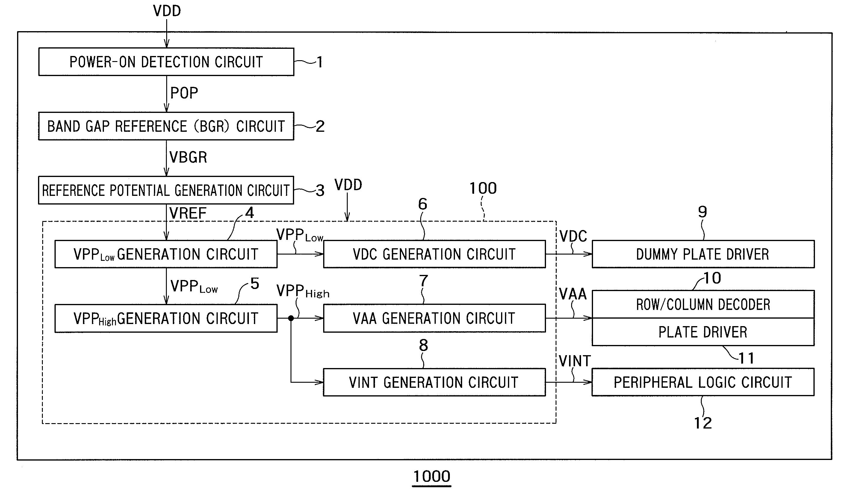
[0056]FIG. 1 is a block diagram showing an example of a memory system 1000 including an internal power supply voltage generation circuit 100 according to a first embodiment which is a mode of the present invention.

[0057]As shown in FIG. 1, the memory system 1000 includes a power-on detection circuit 1, a band gap reference (BGR) circuit 2, a reference potential generation circuit 3, a VPPLow generation circuit (charge pump circuit) 4, a VPPHigh generation circuit (charge pump circuit) 5, a VDC generation circuit (voltage stepdown circuit) 6, a VAA generation circuit (voltage stepdown circuit) 7, a VINT generation circuit (voltage stepdown circuit) 8, a dummy plate driver 9, a row / column decoder 10, a plate driver 11, and a peripheral logic circuit 12.

[0058]The internal power supply voltage generation circuit 100 includes the VPPLow generation circuit (charge pump circuit) 4, the VPPHigh generation circuit (charge pump circuit) 5, the VDC generation circuit (voltage stepdown circuit)...

second embodiment

[0111]In the first embodiment, an example of a configuration such that a circuit scheme called PMOS-Feed-Back type is adopted in the circuit configuration of the voltage stepdown circuits in the memory system has been described.

[0112]In a second embodiment, an example in which a scheme called voltage stepdown transistor (giant transistor) is adopted in the circuit configuration of the voltage stepdown circuits in the memory system will be described. The memory system in the present second embodiment has a configuration similar to that of the memory system 1000 in the first embodiment shown in FIG. 1. Furthermore, since operation of the memory system 1000 in the present second embodiment is similar to that in the first embodiment, signal waveforms become similar to those in the first embodiment shown in FIG. 9.

[0113]FIG. 11 is a circuit diagram showing another example of the configuration of the VDC generation circuit (voltage stepdown circuit) 6 shown in FIG. 1. FIG. 12 is a circuit...

third embodiment

[0136]In the first embodiment, the case where the stepped up voltage VPPLow and the stepped up voltage VPPHigh rise at the same time has been described. In the first embodiment, the VPPLow generation circuit causes the VDC potential to rise concurrently with supplying charge to the VPPHigh generation circuit. Therefore, a heavy load is imposed on the VPPLow generation circuit.

[0137]In a third embodiment, therefore, another operation of the memory system 1000 will be described.

[0138]The memory system according to the third embodiment has a configuration similar to that in the memory system 1000 according to the first embodiment shown in FIG. 1.

[0139]FIG. 14 is a diagram showing an example of a configuration of a reference potential generation circuit applied to the band gap reference (BGR) circuit and the reference potential generation circuit showing in FIG. 1.

[0140]As shown in FIG. 14, the potential generation circuits 2 and 3 are circuits which generate the reference voltage VREF ...


PUM


Abstract

An internal power supply voltage generation circuit 100 has a first charge pump circuit which steps up the external power supply voltage in response to the first clock signal and outputs a first stepped up voltage from the first voltage stepup output terminal; a second charge pump circuit which steps up the first stepup voltage in response to the second clock signal and outputs a second stepped up voltage from the second voltage stepup output terminal, the second stepped up voltage being higher than the first stepped up voltage; a first voltage stepdown circuit which steps down the first stepped up voltage and outputs a first stepped down voltage; and a second voltage stepdown circuit which steps down the second stepped up voltage and outputs a second stepped down voltage, the second stepped down voltage being higher than the first stepped up voltage.

Description

CROSS-REFERENCE TO RELATED APPLICATIONS[0001]This application is based upon and claims the benefit of priority from the prior Japanese Patent Application No. 2009-67441, filed on Mar. 19, 2009, and No. 2010-020378, filed on Feb. 1, 2010, the entire contents of which are incorporated herein by reference.BACKGROUND OF THE INVENTION[0002]1. Field of the Invention[0003]The present invention relates to an internal power supply voltage generation circuit applied to LSI circuits such as semiconductor memories of which low voltage operation is required.[0004]2. Background Art[0005]In recent years, for LSI circuits such as semiconductor memories, a power supply which outputs a lower voltage is demanded. And the output voltage of the power supply is lowered although the threshold voltage cannot be scaled by existence of leak currents in the LSI circuits.[0006]Accordingly, it is considered to step up an external power supply voltage by using a voltage stepup (boost) circuit and generate an int...

Claims


Application Information

Patent Timeline
IPC IPC(8): G05F1/10
CPCG05F1/56H02M2003/072H02M3/07G05F3/30H02M3/072
Inventor OGIWARA, RYUTAKASHIMA, DAISABURO
Owner KK TOSHIBA
Why Eureka
Try Eureka