Semiconductor device including transistor whose gate is electrically connected to capacitor

a technology of semiconductor devices and capacitors, applied in pulse generators, pulse techniques, instruments, etc., can solve the problems of difficult semiconductor devices, sample-and-hold circuits, and difficulty in increasing the voltage to be applied to gates

Active Publication Date: 2016-06-28
SEMICON ENERGY LAB CO LTD
View PDF9 Cites 8 Cited by
  • Summary
  • Abstract
  • Description
  • Claims
  • Application Information

AI Technical Summary

Benefits of technology

[0008]An object of one embodiment of the present invention is to provide a semiconductor device having a novel structure that can hold a bias voltage without decreasing the bias voltage, and a signal generation device including the semiconductor device. Another object of one embodiment of the present invention is to provide a semiconductor device having a novel structure that can extend a hold period of a bias voltage that has been temporarily held, and a signal generation device including the semiconductor device.
[0010]One embodiment of the present invention provides a structure in which electric charge is stored, in accordance with a bias voltage, in a gate of a transistor performing switching operation between an input terminal and an output terminal, and the gate is brought into an electrically floating state at the time of completing the storage of electric charge in the gate. One electrode of a capacitor is connected to the gate in an electrically floating state, and the potential of the other electrode of the capacitor is increased, whereby capacitive coupling occurs; thus, the voltage of the gate is increased. The potential of the gate of the transistor is increased, and the bias voltage is sampled without being decreased.
[0011]In one embodiment of the present invention, each of the transistor performing switching operation and a transistor connected to the gate of the transistor is a transistor with an extremely low off-state current. A transistor in which a channel is formed in an oxide semiconductor film can be used as the transistor with an extremely low off-state current. The transistor including an oxide semiconductor is used as a switch, whereby the switch can have a high tolerance to an increased voltage, and the number of elements for increasing a tolerance to a voltage can be small. Furthermore, the amount of electric charge leaking through the switch in an off state is extremely small, achieving excellent bias voltage hold characteristics.
[0019]One embodiment of the present invention can provide a semiconductor device having a novel structure that can hold a bias voltage without decreasing the bias voltage, and a signal generation device including the semiconductor device. One embodiment of the present invention can provide a semiconductor device having a novel structure that can extend a period in which a generated voltage is sampled, and a signal generation device including the semiconductor device.

Problems solved by technology

However, there are problems as follows, for example.
Therefore, it is difficult to increase a voltage to be applied to a gate in the case where a bootstrap circuit which is not improved is used in a semiconductor device such as a sample-and-hold circuit.
Thus, it is difficult for the semiconductor device like the sample-and-hold circuit to hold a bias voltage without decreasing the bias voltage.
Furthermore, it is difficult to hold the bias voltage, which has been temporarily held, for a long period of time because of a leakage current via a transistor.

Method used


Image

  • Semiconductor device including transistor whose gate is electrically connected to capacitor
  • Semiconductor device including transistor whose gate is electrically connected to capacitor
  • Semiconductor device including transistor whose gate is electrically connected to capacitor

Examples


embodiment 1

[0043]In this embodiment, a circuit structure and operation of a semiconductor device are described.

[0044]Note that the semiconductor device is a circuit utilizing semiconductor characteristics. Here, a semiconductor device means a device including a semiconductor element. The term “semiconductor device” includes a driver circuit or the like for driving a circuit including a semiconductor element. In particular, in this specification, the semiconductor device is a circuit that serves as a sample-and-hold circuit.

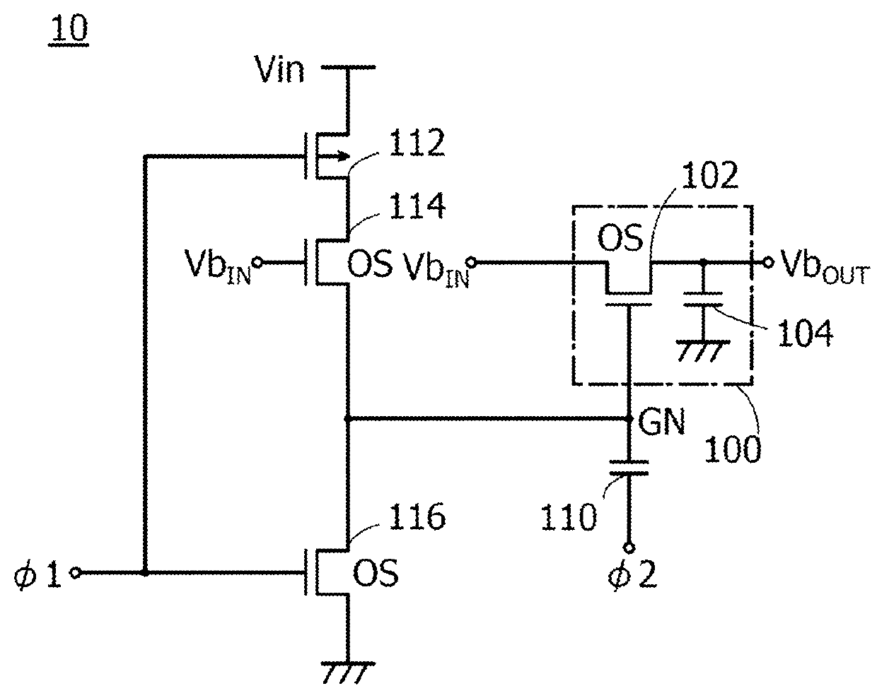
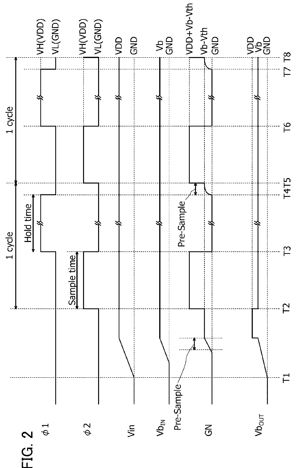
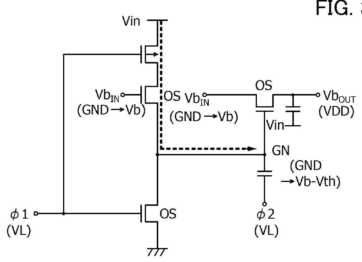
[0045]FIG. 1 illustrates an example of a semiconductor device.

[0046]A semiconductor device 10 illustrated in FIG. 1 includes a transistor 102, a capacitor 104, a capacitor 110, a transistor 112, a transistor 114, and a transistor 116. Note that the transistor 102 and the capacitor 104 are also collectively referred to as a voltage hold portion 100.

[0047]The semiconductor device 10 is supplied with a power supply voltage, a bias voltage, a first control signal (abbreviated to...

embodiment 2

[0100]In this embodiment, a specific example of a structure of a signal generation device including the semiconductor device 10 described in Embodiment 1 is described. Description below is made with reference to FIG. 6, FIG. 7, FIG. 8, FIGS. 9A and 9B, and FIGS. 10A and 10B.

[0101]FIG. 6 illustrates an example of a block diagram of a signal generation device 40 including the semiconductor device 10 illustrated in FIG. 1.

[0102]Note that the signal generation device is a device which generates and outputs a signal in accordance with a signal, a current, or a voltage that are input thereto. Specific examples of the signal generation device include a triangle wave generation circuit and an operational amplifier.

[0103]The signal generation device 40 illustrated in FIG. 6 includes the semiconductor device 10, a bias voltage generation portion 20, and a signal output portion 30. Furthermore, in FIG. 6, a reference bias generation circuit (abbreviated to “BIASGEN” in the drawing) 50 that sup...

embodiment 3

[0154]In this embodiment, an oxide semiconductor layer that can be used for the semiconductor layer to be a channel formation region of the transistor with low off-state current described in the above embodiment is described.

[0155]An oxide semiconductor used for the semiconductor layer to be a channel formation region of the transistor preferably contains at least indium (In) or zinc (Zn). In particular, In and Zn are preferably contained. A stabilizer for strongly bonding oxygen is preferably contained in addition to In and Zn. As a stabilizer, at least one of gallium (Ga), tin (Sn), zirconium (Zr), hafnium (Hf), and aluminum (Al) may be contained.

[0156]As another stabilizer, one or plural kinds of lanthanoid such as lanthanum (La), cerium (Ce), praseodymium (Pr), neodymium (Nd), samarium (Sm), europium (Eu), gadolinium (Gd), terbium (Tb), dysprosium (Dy), holmium (Ho), erbium (Er), thulium (Tm), ytterbium (Yb), and lutetium (Lu) may be contained.

[0157]As the oxide semiconductor us...


PUM


Abstract

Electric charge is stored, in accordance with a bias voltage, in a gate of a transistor performing switching operation between an input terminal and an output terminal, and the gate is brought into an electrically floating state at the time of completing the storage of electric charge in the gate. One electrode of a capacitor is connected to the gate in an electrically floating state, and the potential of the other electrode of the capacitor is increased, so that the voltage of the gate is increased using capacitive coupling. The potential of the gate of the transistor is increased, and the bias voltage is sampled without being decreased. Each of the transistor performing switching operation and a transistor connected to the gate of the transistor is a transistor with an extremely low off-state current.

Description

BACKGROUND OF THE INVENTION[0001]1. Field of the Invention[0002]The present invention relates to an object, a method, or a manufacturing method. The present invention relates to a process, a machine, manufacture, or a composition of matter. One embodiment of the present invention relates to a semiconductor device, a display device, a light-emitting device, a power storage device, a driving method thereof, or a manufacturing method thereof. In particular, one embodiment of the present invention relates to a semiconductor device or a signal generation device including the semiconductor device.[0003]2. Description of the Related Art[0004]A bootstrap circuit that generates a voltage higher than or equal to a power supply voltage using capacitive coupling is known (see Patent Document 1).REFERENCEPatent Document[0005][Patent Document 1] PCT International Publication No. 2006 / 096748SUMMARY OF THE INVENTION[0006]It is necessary to consider the tolerance to an increased voltage in the case ...

Claims


Application Information

Patent Timeline
Patent Type & Authority Patents(United States)
IPC IPC(8): G11C27/02H03K17/16H01L27/06
CPCG11C27/024H01L27/0688H01L27/1225H01L27/124H01L27/1251H01L27/1255H01L29/78651H01L29/7869H03F1/0233H03F3/45273H03F2200/555H03F2203/45288H03K4/06
Inventor TAKAHASHI, KEI
Owner SEMICON ENERGY LAB CO LTD
Why Eureka
Try Eureka