Nvsram cells with voltage flash charger

a technology of nvsram cells and flash chargers, applied in the field of n, can solve the problems of the large size of the 12 t nmos nvsram memory, and achieve the effects of saving more cell size, long channel length, and big overhead

Inactive Publication Date: 2014-05-01
APLUS FLASH TECH
View PDF4 Cites 8 Cited by
  • Summary
  • Abstract
  • Description
  • Claims
  • Application Information

AI Technical Summary

Benefits of technology

[0040]During NVSRAM's Recall operation, the flash part of this pseudo-10 T NVSRAM cell is configured into a paired voltage followers with their respective drain voltages preferably supplied by the coupling-generated charges rather than by the current supply from the VDD

Problems solved by technology

One big drawback of this 12 T NMOS NVSRAM memory is its large 12 T ce

Method used


Image

  • Nvsram cells with voltage flash charger
  • Nvsram cells with voltage flash charger
  • Nvsram cells with voltage flash charger

Examples


Embodiment Construction

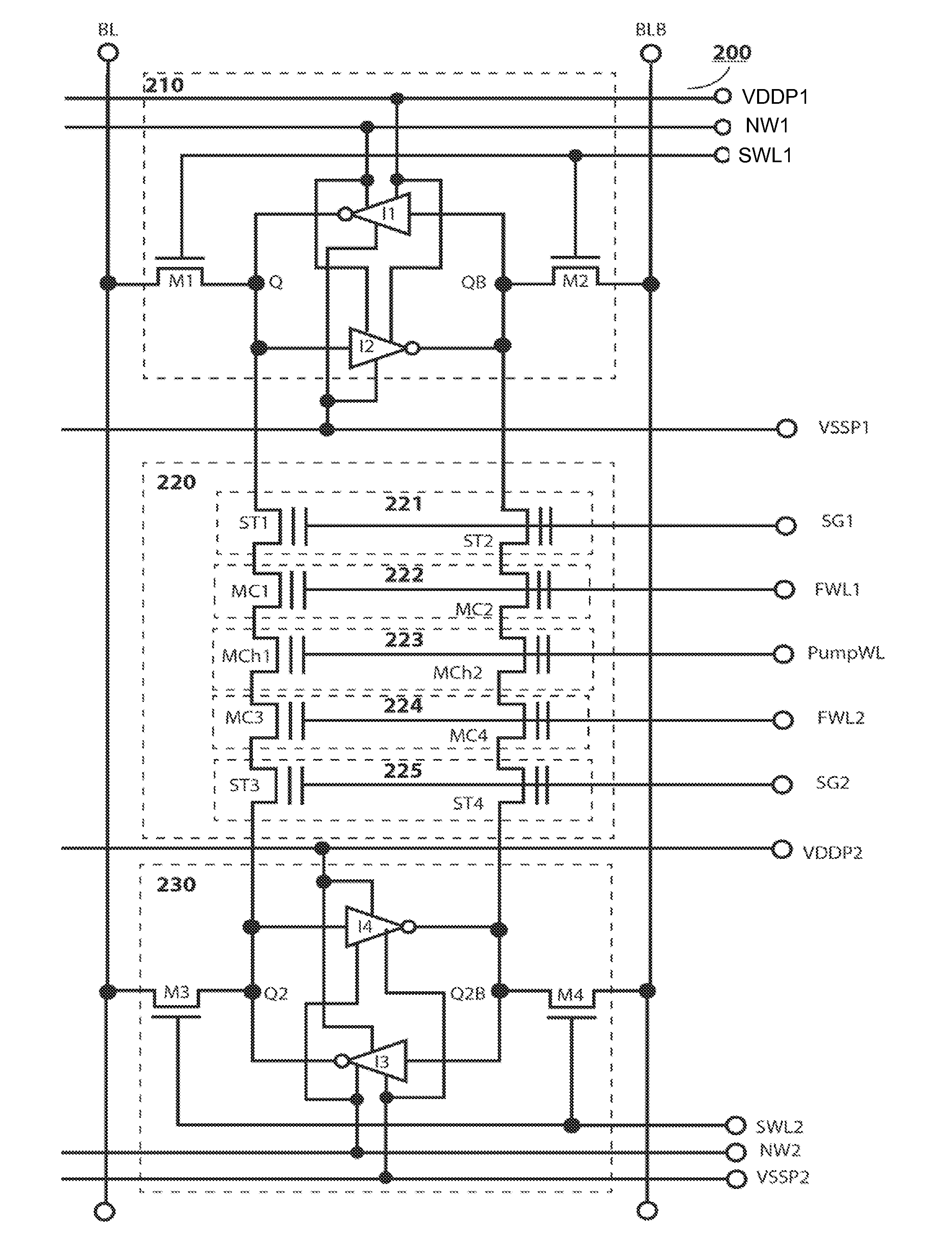
[0051]The present invention relates to a preferred 12 T NVSRAM cell with a Flash Charger or a pseudo-10 T NVSRAM cell comprising one LV 6 T SRAM cell, one 4 T Flash cell and one shared paired Flash Charger transistors (2 T) that can be made of a conventional 2-poly Flash transistor or a 1-poly Select transistor by shorting poly2 and poly1 of the flash cell. These shared 2 T Flash Charger transistors are formed on available room of layout spacing between two source nodes of two 10 T NVSRAM cells laid in same column without taking extra silicon area. Thus, this preferred pseudo-10 T NVSRAM cell makes a cell size of the 12 T NVSRAM cell with a Flash Charger effectively equivalent to a 10 T cell.

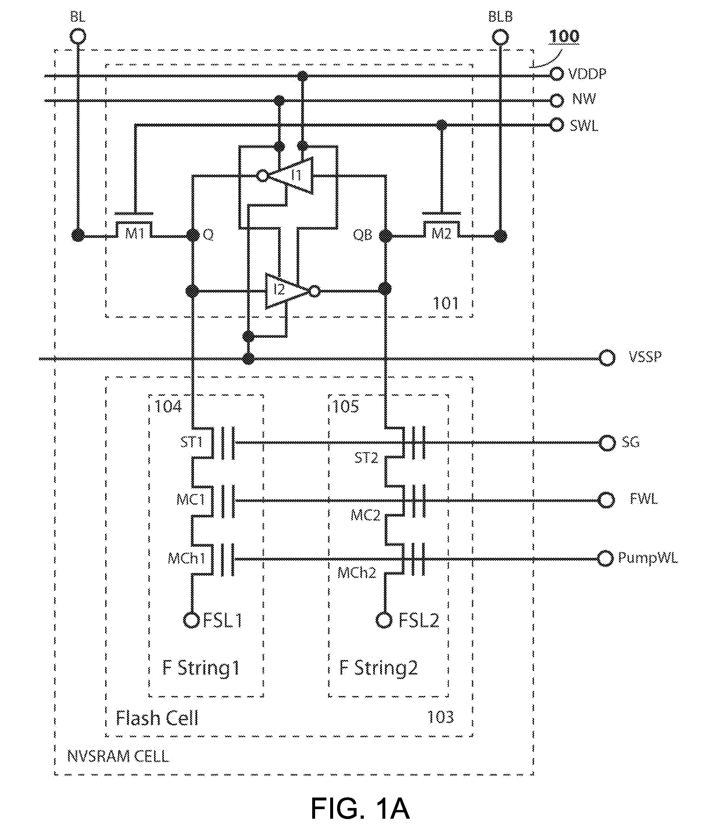
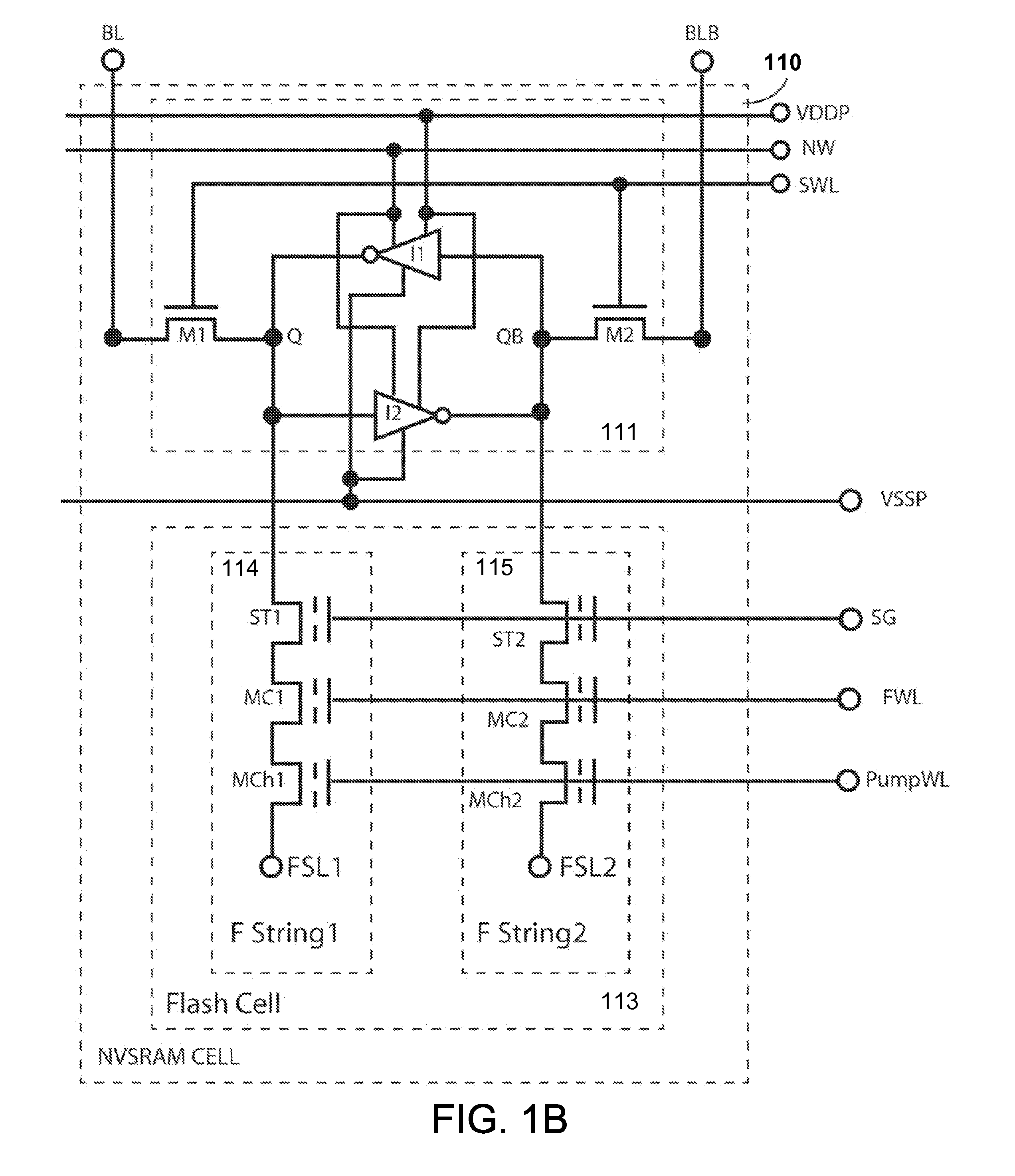
[0052]FIG. 1A shows a preferred embodiment of a 2-poly NMOS 12 T NVSRAM cell with a Flash-based Charger of the present invention. Each 12 T NVSRAM cell with a Flash Charger 100 includes one 6 T LV SRAM cell 101 and one 6 T NMOS 2-poly Flash cell 103. Each 6 T LV SRAM cell 101 is like conventiona...


PUM


Abstract

The present invention discloses two preferred embodiments of a 12 T NVSRAM cell with a flash-based Charger and a pseudo 10 T NVSRAM cell with one shared Flash-based Charger. The Flash-based Charger can be made of a 2-poly floating-gate type or a 1-poly charge-trapping SONOS/MONOS flash type, regardless of PMOS type or NMOS type. In an alternative embodiment, the Store operation of above two preferred NVSRAM cell use a DRAM-like charge-sensing scheme with Flash cell configured into a voltage follower associated with Flash Charger and 2-step SRAM amplification technique to amplify the threshold level difference ΔVt stored in the paired Flash transistors. The ΔVt can be detected as low as 1V when the coupled charges through the Flash charger are sufficient by ramping a gate control of the Flash Charger as high as VPP or by increasing the channel length for the Flash Charger.

Description

CROSS-REFERENCE TO RELATED APPLICATIONS[0001]This application claims priority to U.S. Patent Application No. 61 / 721,467, filed on Nov. 1, 2012, commonly assigned, and hereby incorporated by references in their entireties herein for all purposes.[0002]This application is related to U.S. Pat. No. 7,164,608, U.S. patent application Ser. Nos. 14 / 037,356, 14 / 053,549, 14 / 058,227, 14 / 059,618, and 14 / 064,220, commonly assigned, which are incorporated by reference herein for all purposes.[0003]Additionally, this application is related to U.S. Pat. No. 7,760,540.TECHNICAL FIELD OF THE INVENTION[0004]The present invention relates to a 12 T NVSRAM cell with a flash Charger comprising one LV 6 T SRAM cell, one 4 T Flash cell and one shared paired Flash Charger transistors (2 T) that can be made of a conventional 2-poly Flash transistor or a 1-poly Select transistor by shorting poly2 and poly1 of the flash cell. Additionally, the invention also provides a pair of mirrored 10 T NVSRAM cells with a...

Claims


Application Information

Patent Timeline
IPC IPC(8): G11C14/00
CPCG11C14/0063
Inventor LEE, PETER WUNG
Owner APLUS FLASH TECH
Why Eureka
Try Eureka