
Method and circuit arrangement for accessing slave units in a system on chip in a controlled manner

a slave unit and control method technology, applied in the field of electronic and logic circuits, can solve the problem of terminating the master unit's unauthorized access in the network-on-chip bus system, and achieve the effect of simple manner, no additional overhead, and little or no access time delay

Inactive Publication Date: 2016-01-07
SIEMENS AG
View PDF22 Cites 16 Cited by
  • Summary
  • Abstract
  • Description
  • Claims
  • Application Information

AI Technical Summary

Benefits of technology

The invention provides a method and circuit arrangement to control accesses between master and slave units in a system on chip without additional overheads. This method and arrangement can prevent unauthorized accesses and minimize additional latency or time delay caused by checking access authorizations. It is simple and efficient, and does not impair the performance and efficiency of the system on chip. The invention allows for the control of accesses without changing or enhancing IP blocks or the network-on-chip bus system. Overall, the invention provides a way to securely protect unauthorized accesses in a simple and effective manner.

Problems solved by technology

It is also unnecessary, e.g., to enhance the existing network-on-chip system with additional control functionality to recognize and prevent unauthorized accesses.
Consequently, the unauthorized access of the master unit is terminated in the network-on-chip bus system, because the access cannot be forwarded to any slave unit as a destination unit.

Method used


Image

  • Method and circuit arrangement for accessing slave units in a system on chip in a controlled manner
  • Method and circuit arrangement for accessing slave units in a system on chip in a controlled manner
  • Method and circuit arrangement for accessing slave units in a system on chip in a controlled manner

Examples


Embodiment Construction

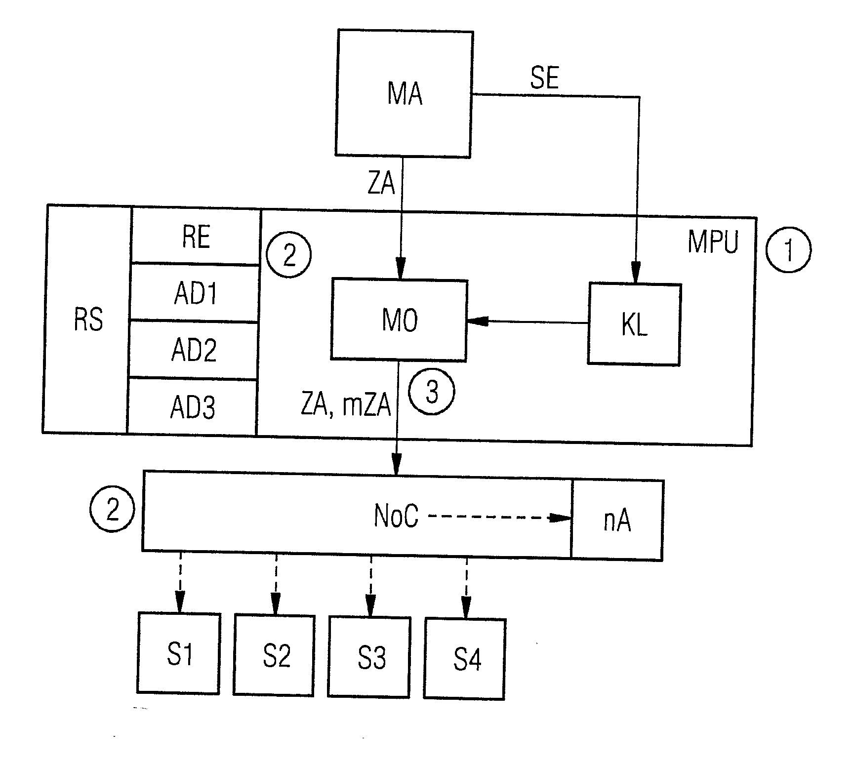
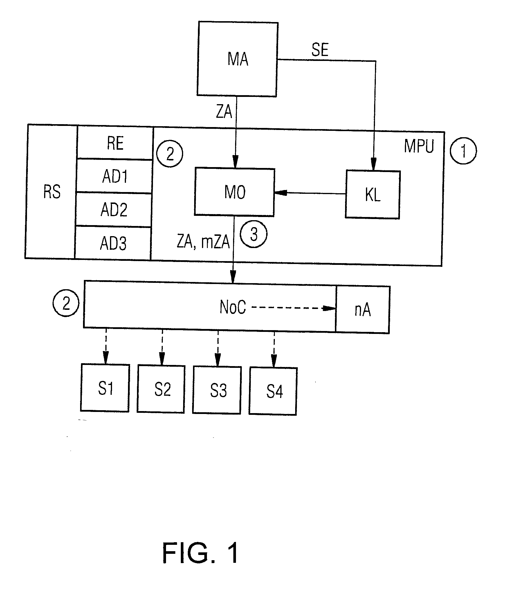
[0031]In an exemplary and schematic manner, FIG. 1 shows a circuit arrangement for performing the inventive method for controlled accesses by at least one master unit MA to at least one slave unit S1, S2, S3, S4 in a system on chip. The exemplary circuit arrangement is at least part of the system on chip. In addition to the circuit arrangement shown, the system on chip may comprise further components or IP units, such as a control unit or CPU, input and output units, and further master units (e.g., coprocessors). For the sake of simplicity, however, these components or IP units are not shown.

[0032]The inventive circuit arrangement includes at least one master unit MA, such as a direct memory access of a peripheral unit, controller, or coprocessor, and at least one slave unit S1, S2, S3, S4. A slave unit S1, S2, S3, S4 may be, e.g., a peripheral unit, an input / output unit, or a memory unit or memory area. A master unit MA may have, e.g., write access, read access or execute access to...


PUM


Abstract

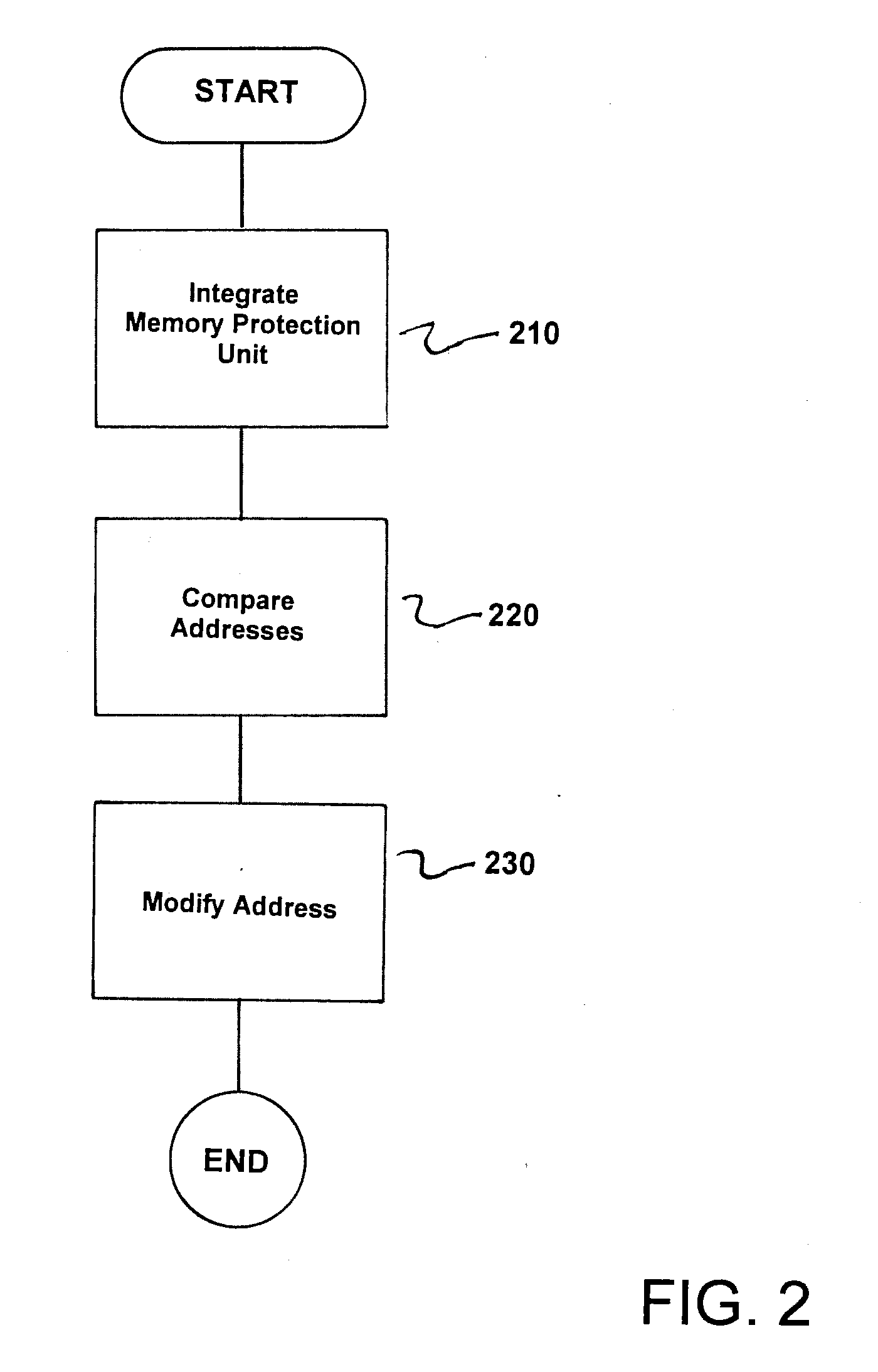
A circuit arrangement and method for accessing slave units in a system on chip in a controlled manner, wherein an access of a master unit of the system on chip to one of the slave units is performed via a network-on-chip bus system using an access address, where a memory protection unit is integrated between the at least one master unit and the network-on-chip bus system, and access authorization of the master unit to a slave unit is checked by the memory protection unit by comparing the access address with specified address sections, and when an unauthorized access of the master unit to a slave unit is identified, the access address is modified by the memory protection unit such that the unauthorized access is terminated in the network-on-chip bus system.

Description

CROSS-REFERENCE TO RELATED APPLICATIONS[0001]This is a U.S. national stage of application No. PCT / EP2014 / 052702 filed 12 Feb. 2014. Priority is claimed on German Application No. 10 2013 203 365.6 filed 28 Feb. 2013, the content of which is incorporated herein by reference in its entirety.BACKGROUND OF THE INVENTION[0002]1. Field of the Invention[0003]The present invention generally relates to the field of electronic and logic circuits and, more particularly, to the field of application-specific integrated circuits (ASICs). Specifically, the present invention relates to a method for accessing slave units in a system on chip in a controlled manner, and to an associated circuit arrangement. Having at least one master unit, a plurality of subordinate slave units, and a network-on-chip bus system (NoC), where an access of a master unit to a slave unit is effected by an access address via the network-on-chip bus system.[0004]2. Description of the Related Art[0005]Logic and / or electronic c...

Claims


Application Information

Patent Timeline
Patent Type & Authority Applications(United States)
IPC IPC(8): G06F13/364G06F12/14G06F13/40G06F13/42
CPCG06F12/1425G06F13/364G06F2212/1052G06F13/404G06F13/4282G06F12/14G06F2213/0038
Inventor EPPENSTEINER, FRIEDRICHGHAMESHLU, MAJIDHAHN, ULRICHTAUCHER, HERBERT
Owner SIEMENS AG
Learn More