Recording element substrate, method of manufacturing the recording element substrate, and liquid ejection head
a technology of recording element and substrate, which is applied in the direction of metal-working equipment, printing, writing implements, etc., can solve the problems of heat storage, degradation of protection film, and degradation of image quality, so as to reduce thermal interference, stable recording, and high reliability
- Summary
- Abstract
- Description
- Claims
- Application Information
AI Technical Summary
Benefits of technology
Problems solved by technology
Method used
Image
Examples
first embodiment
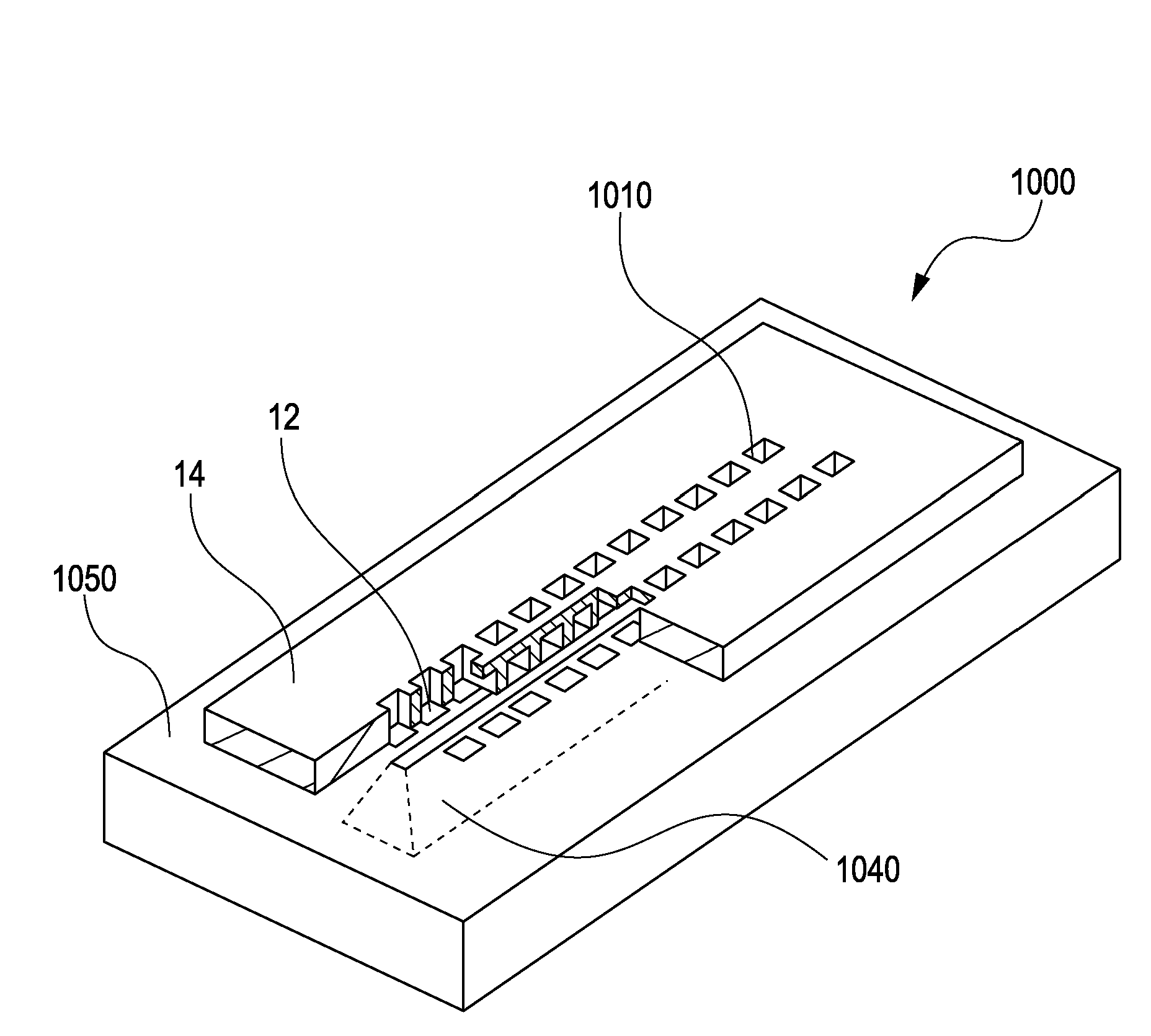
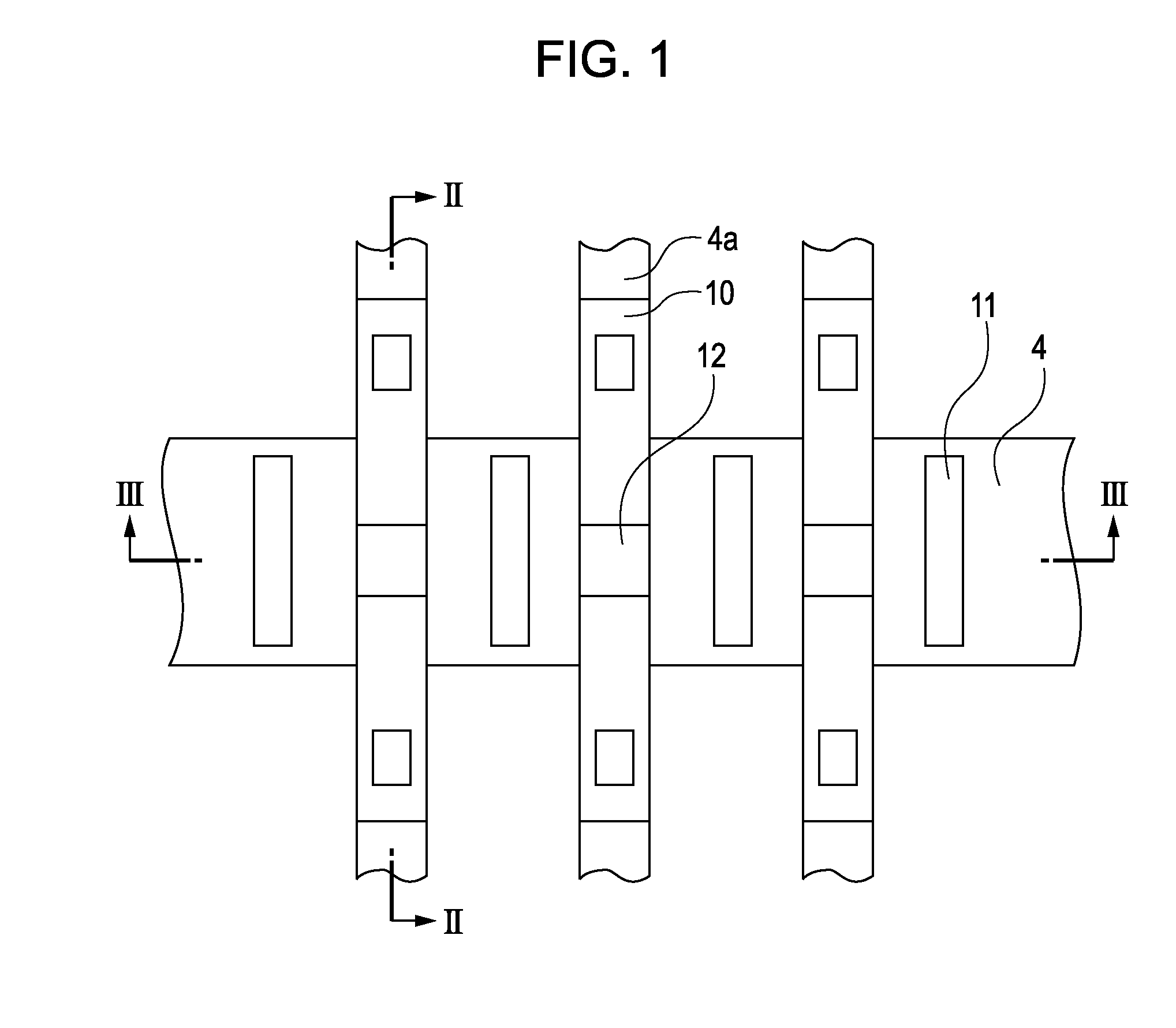
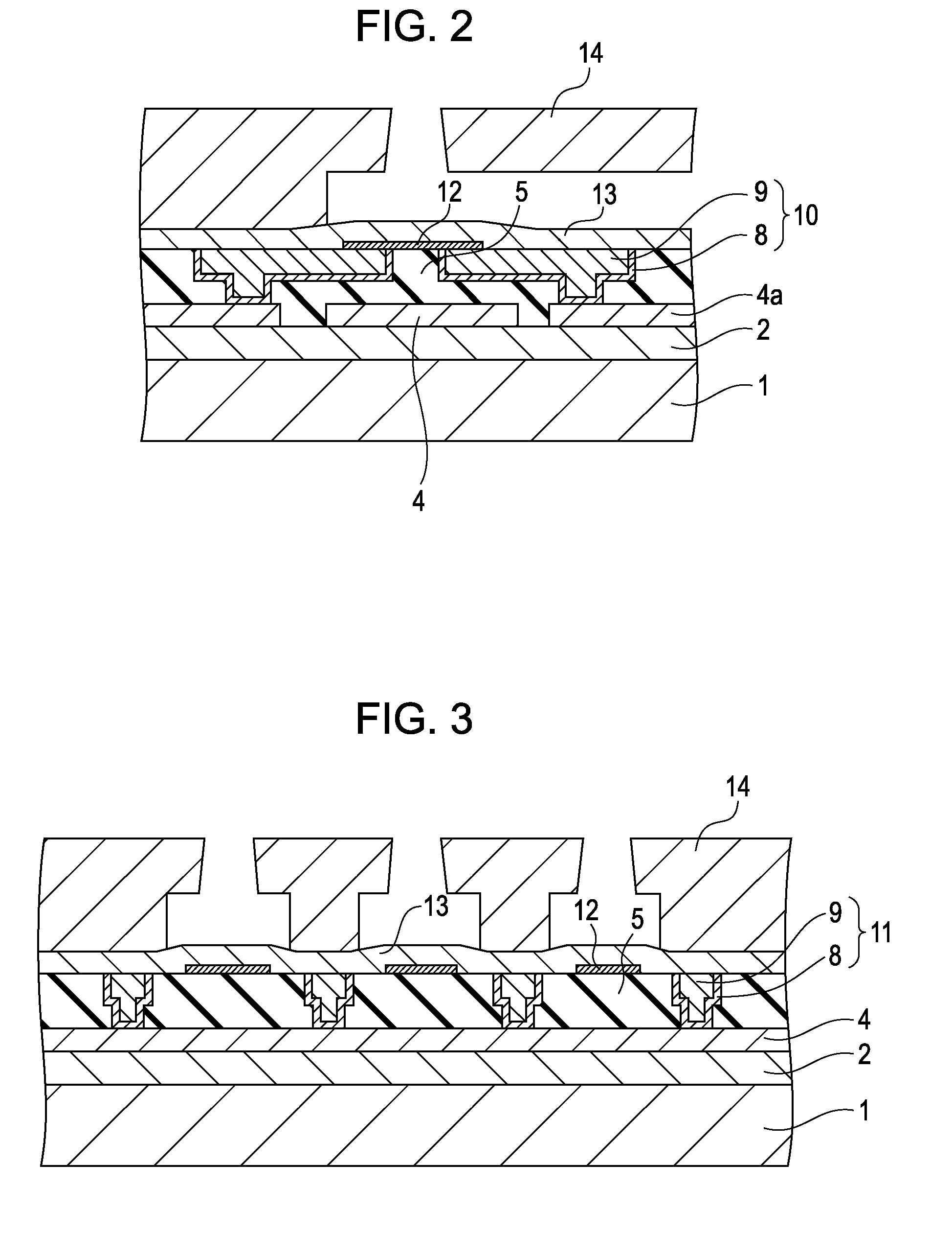
[0038]An embodiment of the present invention will be described with reference to FIGS. 2 and 3. As shown in FIG. 2, an interlayer film 2 composed of boron- and phosphorus-doped SiO2 is disposed at a thickness of 500 nm on a Si substrate 1 provided with active elements, such as transistors (not shown). A heat conduction layer 4 and an electrode layer 4a composed of an Al—Si alloy are disposed at a thickness of 400 nm on the interlayer film 2. An insulating layer 5 composed of SiO2 is disposed at a thickness of 1 μm on the heat conduction layer 4 and the electrode layer 4a. The insulating layer 5 also serves as a heat storage layer that stores the heat of the heating portions 12. The heating portions 12 composed of TaSiN are disposed at a thickness of 50 nm on the insulating layer 5. Both ends of each heating portion 12 are in contact with electrodes 10. The electrodes 10 are in contact with the electrode layer 4a through contact holes provided in the insulating layer 5.
[0039]The elec...
second embodiment
[0053]Examples according to a second embodiment of the present invention are shown in FIGS. 7A and 7B. The structure and the manufacturing method in the second embodiment are the same as those in the first embodiment except for the shape of the heat conduction members 11, and thus, a repeated description thereof will be omitted. As shown in the first embodiment, by providing the heat conduction members 11 as shown in FIG. 1, thermal interference can be prevented. In the case where higher speed is required, adjustment can be made by increasing the volume of the heating portions 12. However, if the distance between each of the heat conduction members 11 and its adjacent heating portion 12 is too small, the insulating layer 5 cannot produce an effect as a heat storage layer, and heat of the heating portion 12 escapes to the heat conduction member 11 before ink is subjected to film boiling. Therefore, it is necessary to locate the heat conduction member 11 at a position at least 1 μm aw...
third embodiment
[0055]Examples according to a third embodiment of the present invention are shown in FIGS. 8A and 8B. The structure and the manufacturing method in the third embodiment are the same as those in the first embodiment except for the shape of the heat conduction members 11, and thus, a repeated description thereof will be omitted.
[0056]FIGS. 8A and 8B are each a schematic plan view showing an end portion of the arrangement of heating portions 12 which are arranged at a predetermined pitch as shown in FIG. 6. In the recording element substrate 1050, since the heating portions 12 are densely located in the central region, heat is more easily stored in the central region than in the end region. When there is a temperature variation between the central region and the end region of the recording element substrate 1050, ink on a heating portion 12 located in the central region is heated faster than ink on a heating portion 12 located in the end region, resulting in a variation in ejection. Su...
PUM
| Property | Measurement | Unit |
|---|---|---|
| Distance | aaaaa | aaaaa |
| Volume | aaaaa | aaaaa |
| Width | aaaaa | aaaaa |
Abstract
Description
Claims
Application Information


