

Electronic device package, module, and electronic device
- Summary
- Abstract
- Description
- Claims
- Application Information
AI Technical Summary
Benefits of technology
Problems solved by technology
Method used
Image

Examples
first exemplary embodiment
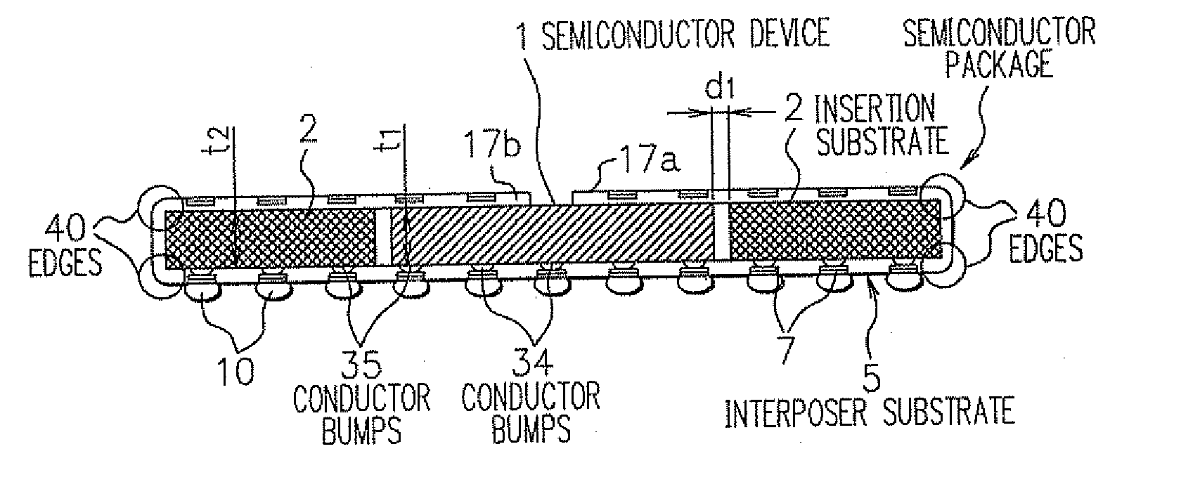
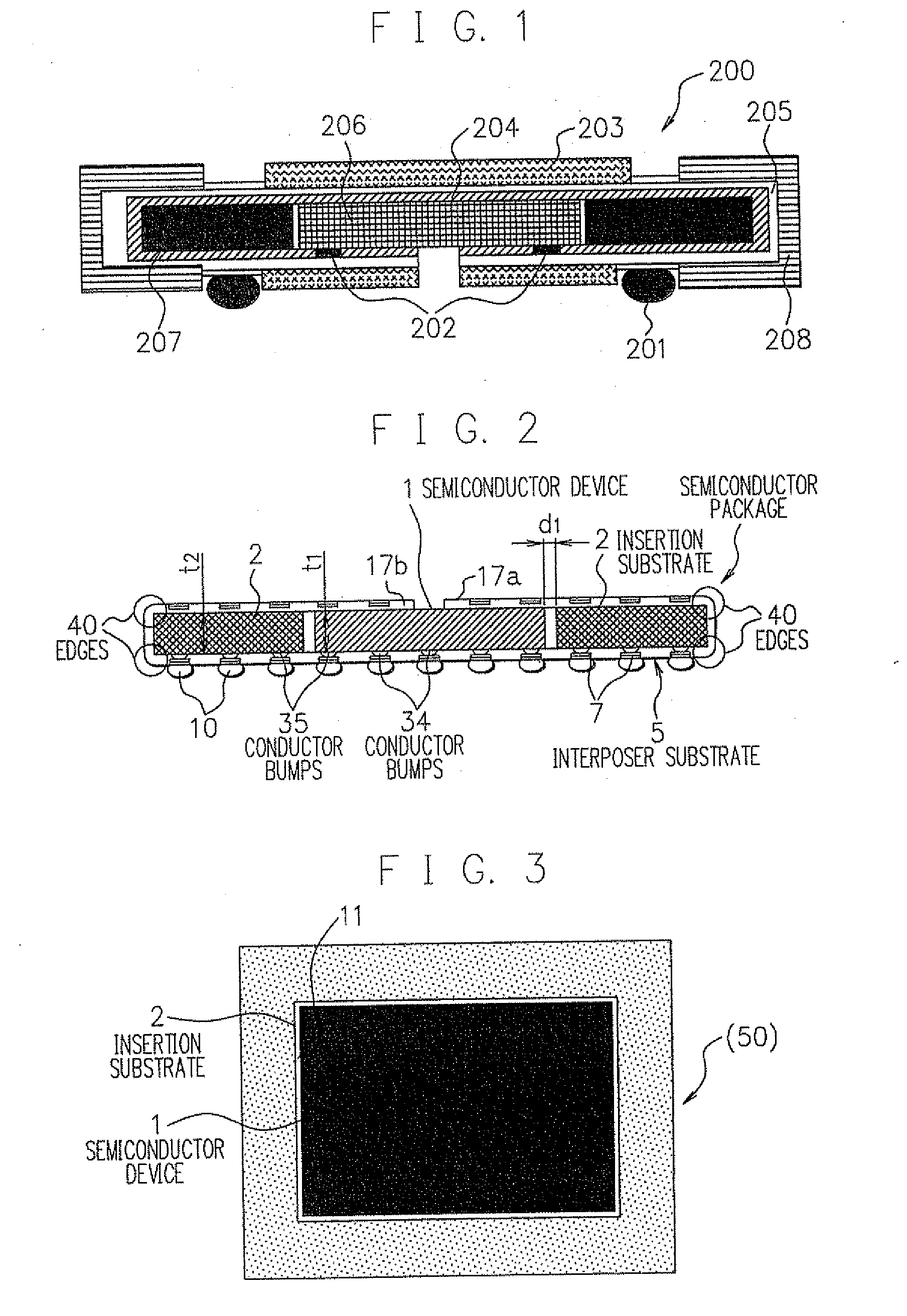
[0019]FIG. 2 is a vertical section of a semiconductor package of a first exemplary embodiment. FIG. 3 is a top view of the semiconductor package of FIG. 2 but an interposer substrate (flexible substrate) is not shown.
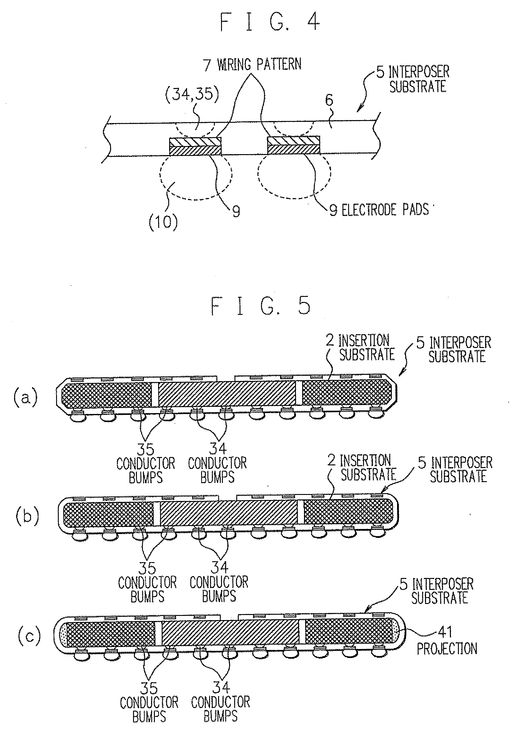
[0020]As shown in FIG. 2, a semiconductor package 50 of the present embodiment includes a semiconductor device (electronic device) 1, an insertion substrate 2 disposed around the semiconductor device 1, and a flexible interposer substrate 5 disposed so as to surround the semiconductor device 1 and the insertion substrate 2. Basically, a known member can be used as each of the members of the semiconductor device 1, the insertion substrate 2, and the interposer substrate 5. A main feature of the present invention is that, as will be described later, a wiring pattern (a ground line or a power supply line) of the interposer substrate 5 is electrically connected to the insertion substrate 2.
[0021]The semiconductor device 1 is constructed by, for example, a CPU, a DRAM, and t...
second exemplary embodiment
[0039]In the first exemplary embodiment, the insertion substrate 2 made of a single member and formed in a frame shape is used. However, the present invention is not limited to the first exemplary embodiment. A configuration as shown in FIG. 7 may be employed. FIG. 7 is a top view of a semiconductor package according to a second exemplary embodiment, in which the interposer substrate is not shown. Configuration examples of the present invention will be described below taking the second to eighth exemplary embodiments as examples. Naturally, it is also possible to properly combine the configurations described in the exemplary embodiments as necessary.
[0040]A semiconductor package 51A shown in FIG. 7A is different from the foregoing embodiment in the point that a pair of insertion substrates 2a and 2b each having a U shape and bilaterally symmetrical are used. The insertion substrates 2a and 2b are disposed so as to face each other and surround the semiconductor device 1. The insertio...
third exemplary embodiment
[0047]In the first exemplary embodiment, the single-layer interposer substrate 5 is used. However, the present invention is not limited to the first exemplary embodiment. A multilayer interposer substrate 15 may be employed as shown in FIG. 10. A semiconductor package 52 in FIG. 10 is obtained by changing only the interposer substrate 5 in the package of the first exemplary embodiment, and the other structure is the same as that in the first exemplary embodiment.
[0048]The interposer substrate 15 is a two-layer-type wiring substrate including a second wiring pattern 8 in addition to the first wiring pattern 7. Even in the case of using the interposing substrate 15 of the two-layer type (or three or more layer type), by connecting the ground line (or the power supply line) of the wiring patterns 7 and 8 to the insertion substrate 2, enhancement of the ground line (or enhancement of the power supply line) is realized in a manner similar to the first exemplary embodiment.
[0049]In the pr...
PUM
 Abstract
Description
Claims
Application Information