
Polishing apparatus and polishing method

Active Publication Date: 2010-10-07
EBARA CORP
View PDF17 Cites 6 Cited by
  • Summary
  • Abstract
  • Description
  • Claims
  • Application Information

AI Technical Summary

Benefits of technology

[0009]Meanwhile, compared to the method of using a top ring having a plurality of pressure chambers, air bags, or the like, more precise control of a polishing profile can be performed by a method which comprises supplying a polishing liquid from a polishing liquid supply port (polishing liquid supply position) to a polishing surface while moving the polishing liquid supply port in carrying out polishing. This method, however, necessitates many control parameters. This requires many polishing tests until an intended polishing profile is obtained, which also incurs increased cost of consumables, such as a semiconductor wafer.
[0040]According to the polishing method of the present invention, the consumption of a polishing liquid can be reduced while maintaining a relatively high polishing rate.

Problems solved by technology

This method, however, cannot control the pressure on a smaller area than a pressure chamber, an air bag or the like, making it impossible to control the polishing profile for such small areas.
More precise profile control is thus difficult.
This method, however, necessitates many control parameters.
This requires many polishing tests until an intended polishing profile is obtained, which also incurs increased cost of consumables, such as a semiconductor wafer.
In particular, a polishing liquid (slurry) for use in chemical mechanical polishing (CMP) is not only costly, but also entails a heavy burden on its waste (discharge) treatment.

Method used


Image

  • Polishing apparatus and polishing method
  • Polishing apparatus and polishing method
  • Polishing apparatus and polishing method

Examples


example 1

[0141]In the polishing apparatus shown in FIG. 16, the movement range between the first supply position F and the second supply position S was divided into 11 movement sections (oscillation zones 1 to 11) and the movement speed (oscillation speed) of the polishing liquid supply port (polishing liquid supply position) 108a was set for each movement section as indicated in Table 2 below, and polishing of a semiconductor wafer, having a diameter of 300 mm, was carried out.

TABLE 2From second supply position to first supply positionFrom first supply position to second supply positionCenter →EdgeEdge→ CenterStart PositionEnd PositionOsci. Dist.Osci. SpeedStart PositionEnd PositionOsci. Dist.Osci. Speed[mm][mm][mm][mm / s][mm][mm][mm][mm / s]Oscillation Zone-1195.5177.018.5150.017.717.7130Oscillation Zone-2177.0159.317.71517.735.417.7130Oscillation Zone-3159.3141.617.71535.453.117.7130Oscillation Zone-4141.6123.917.74053.170.817.790Oscillation Zone-5123.9106.217.74070.888.517.790Oscillation Zo...

example 2

[0145]Polishing of a semiconductor wafer, having a diameter of 300 mm, was carried out in the same manner as in Example 1 except that a polishing liquid was supplied at a flow rate of 100 ml / min to the polishing surface 52a from the polishing liquid supply port (polishing liquid supply position) 108a of the polishing liquid supply nozzle 108.

[0146]The polishing rate (Removal Rate) in this polishing is shown in FIG. 23, and the relationship between polishing rate (Removal Rate) and position on the wafer (Wafer Position) in this polishing is shown in FIG. 24. In Comparative Example 4, a semiconductor wafer, having a diameter of 300 mm, was polished in the same manner as in Example 2 except that the polishing liquid supply port 108a of the polishing liquid supply nozzle 108 was kept stationary (fixed) at the first supply position F, the polishing liquid was supplied at a flow rate of 200 ml / min to the polishing surface 52a from the polishing liquid supply port 108a of the polishing liq...


PUM

PropertyMeasurementUnit
Thicknessaaaaaaaaaa
Speedaaaaaaaaaa

Abstract

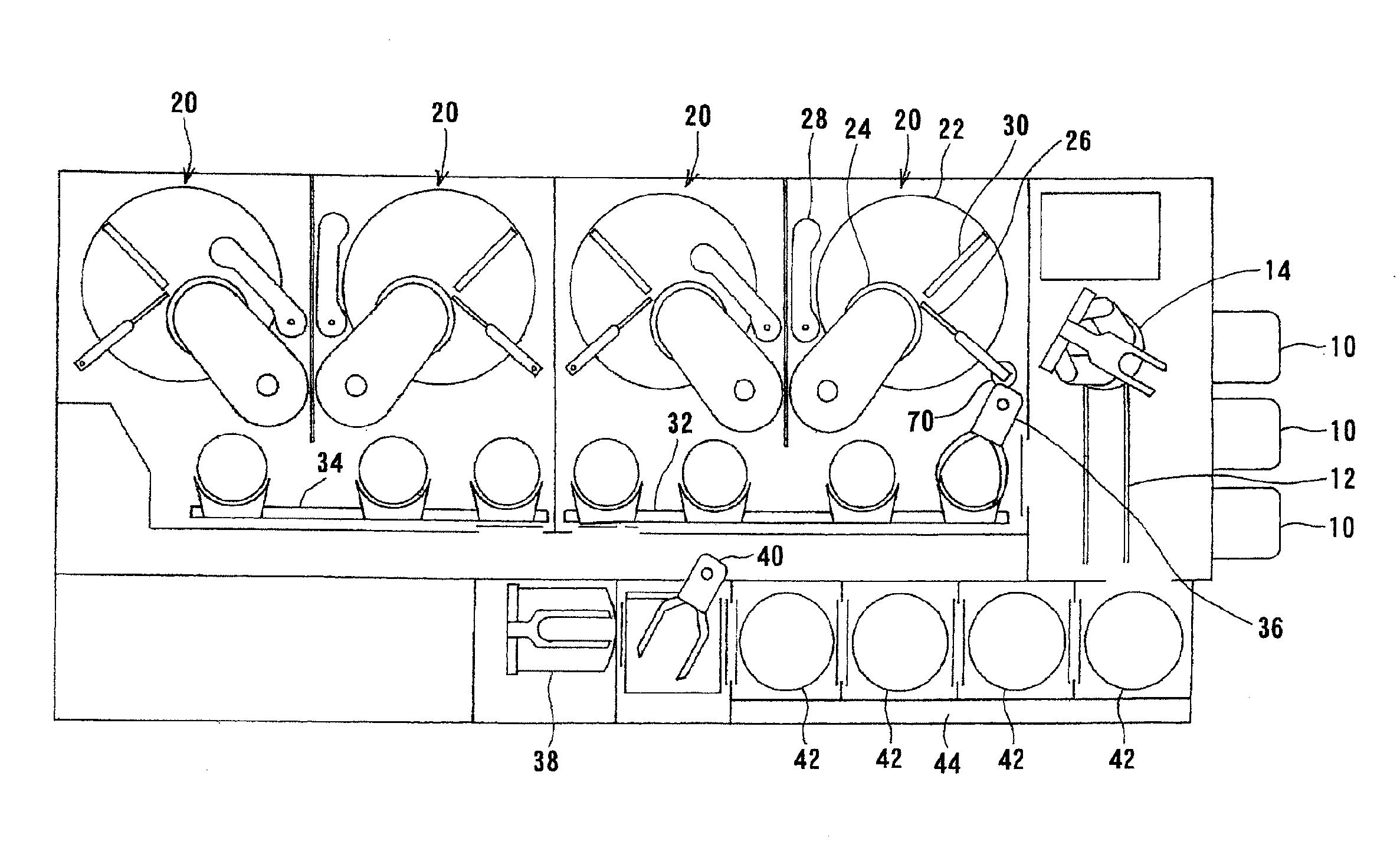
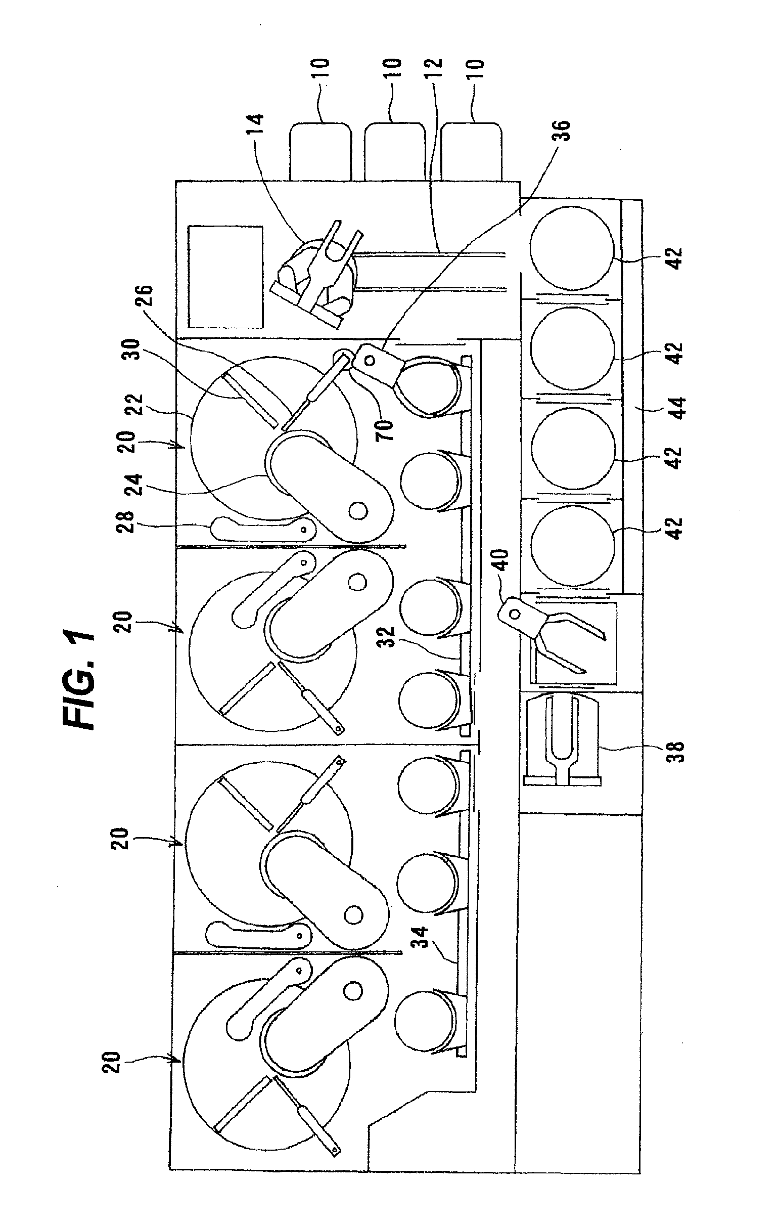
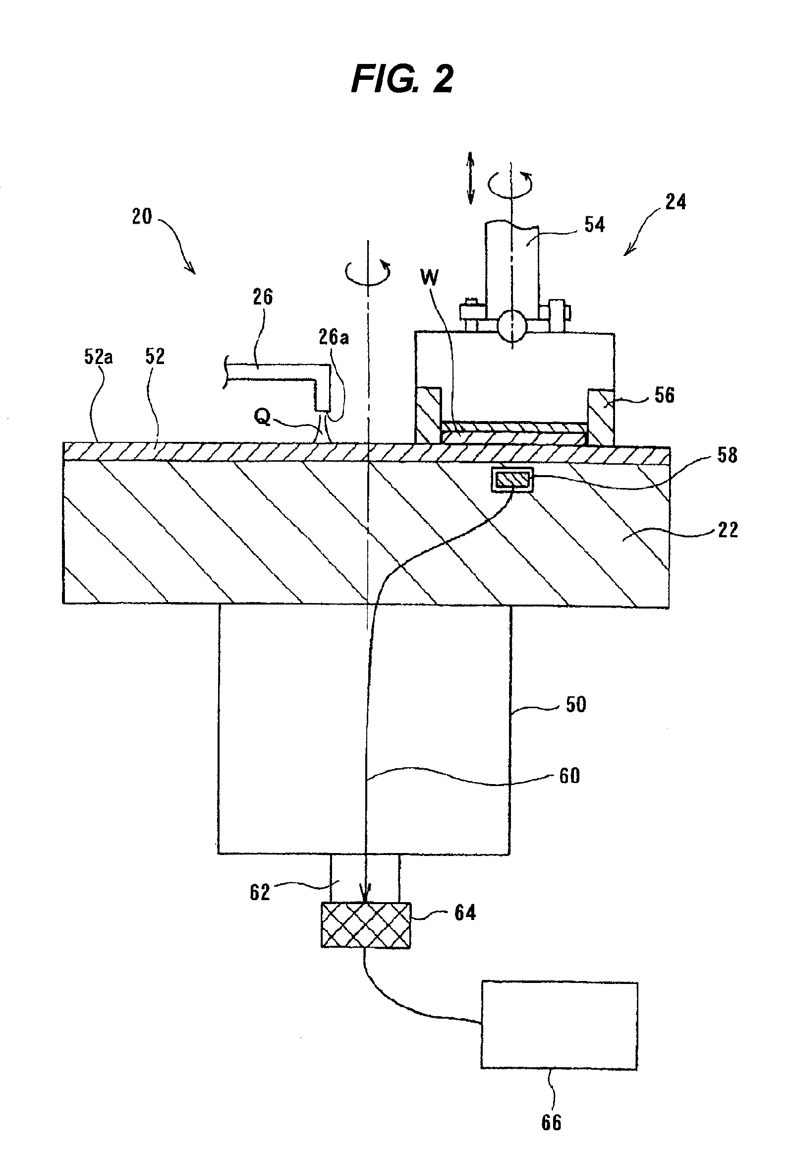
A polishing apparatus can perform more precise control of a polishing profile without carrying out many polishing tests in advance. The polishing apparatus includes: a polishing table 22 having a polishing surface 52a; a top ring 24 for holding a polishing object W and pressing the polishing object W against the polishing surface 52a; a polishing liquid supply nozzle 26 for supplying a polishing liquid to the polishing surface 52a; a movement mechanism 70 for moving a polishing liquid supply position 26a of the polishing liquid supply nozzle 26 approximately along the radial direction of the polishing surface 52a; a controller 66 for controlling the movement mechanism 70; and a simulator 72 for predicting the relationship between the polishing liquid supply position 26a of the polishing liquid supply nozzle 26 and a polishing profile, performing a simulation and outputting data to the controller 66.

Description

BACKGROUND OF THE INVENTION[0001]1. Field of the Invention[0002]The present invention relates to a polishing apparatus and a polishing method, and more particularly to a polishing apparatus and a polishing method for polishing and flattening a polishing object, such as a semiconductor wafer, with the use of a polishing liquid (slurry).[0003]2. Description of the Related Art[0004]With the recent progress toward higher integration of semiconductor devices, circuit interconnects are becoming finer and the distance between adjacent interconnects is becoming smaller. Especially when forming a circuit pattern by optical lithography with a line width of not more than 0.5 μm, a stepper requires a high flatness of imaging surface because of the small depth of focus. A polishing apparatus for carrying out chemical mechanical polishing (CMP) with the use of a polishing liquid is known as such a means for flattening a surface of a semiconductor wafer.[0005]Such a chemical mechanical polishing (...

Claims


Application Information

Patent Timeline
IPC IPC(8): B24B49/00B24B1/00B24B37/04
CPCB24B37/04B24B57/02B24B49/00
Inventor ISHII, YUSHIOKAWA, YOICHIHEIANNA, JYOJIMATSUO, HISANORI
Owner EBARA CORP
Learn More