Semiconductor light-emitting device and manufacturing method of the same

a technology of semiconductors and light-emitting devices, which is applied in the direction of discharge tubes luminescnet screens, television system scanning details, etc., can solve the problems of waste of light traveling in directions different from radiation directions, and not being suitable for mass production, so as to reduce the amount of light

Inactive Publication Date: 2010-10-14
PANASONIC CORP
View PDF5 Cites 133 Cited by
  • Summary
  • Abstract
  • Description
  • Claims
  • Application Information

AI Technical Summary

Benefits of technology

[0016]In the semiconductor light-emitting device of the present invention, the reflective layer is formed on the side surface of the sealant. Thus, light that is emitted from the semiconductor light-emitting element positioned within the sealant is reflected by a reflective surface formed by the boundary surface between the sealant and the reflective layer. This can reduce the amount of light that is emitted from the side surface of the semiconductor light-emitting device, whereby characteristics close to ideal surface emission can be obtained.
[0017]The semiconductor light-emitting device of the present invention can be fabricated by a manufacturing process that is performed in the atmosphere. Moreover, once individual semiconductor light-emitting elements are placed on the submount substrate, the sealant and the reflective layer for the individual semiconductor light-emitting elements can be formed over the submount substrate at a time. Thus, the semiconductor light-emitting device of the present invention is preferable for mass production.

Problems solved by technology

In such cases, light that travels in directions different from the radiation direction is wasted.
However, since forming the reflective layer by the metal thin film or the like requires processing in a vacuum chamber, these examples are not necessarily suitable for mass production.

Method used


Image

  • Semiconductor light-emitting device and manufacturing method of the same
  • Semiconductor light-emitting device and manufacturing method of the same
  • Semiconductor light-emitting device and manufacturing method of the same

Examples


first embodiment

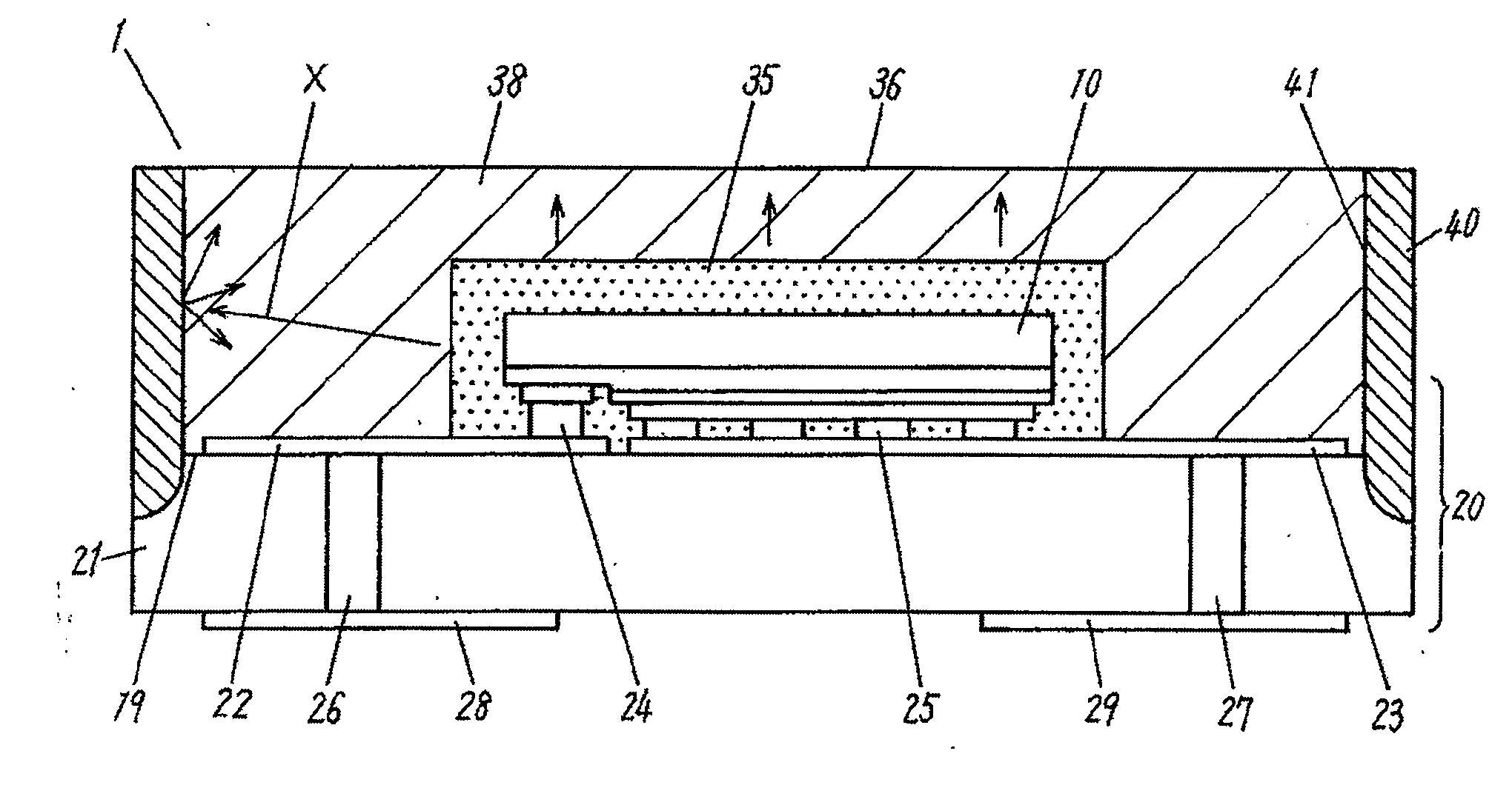
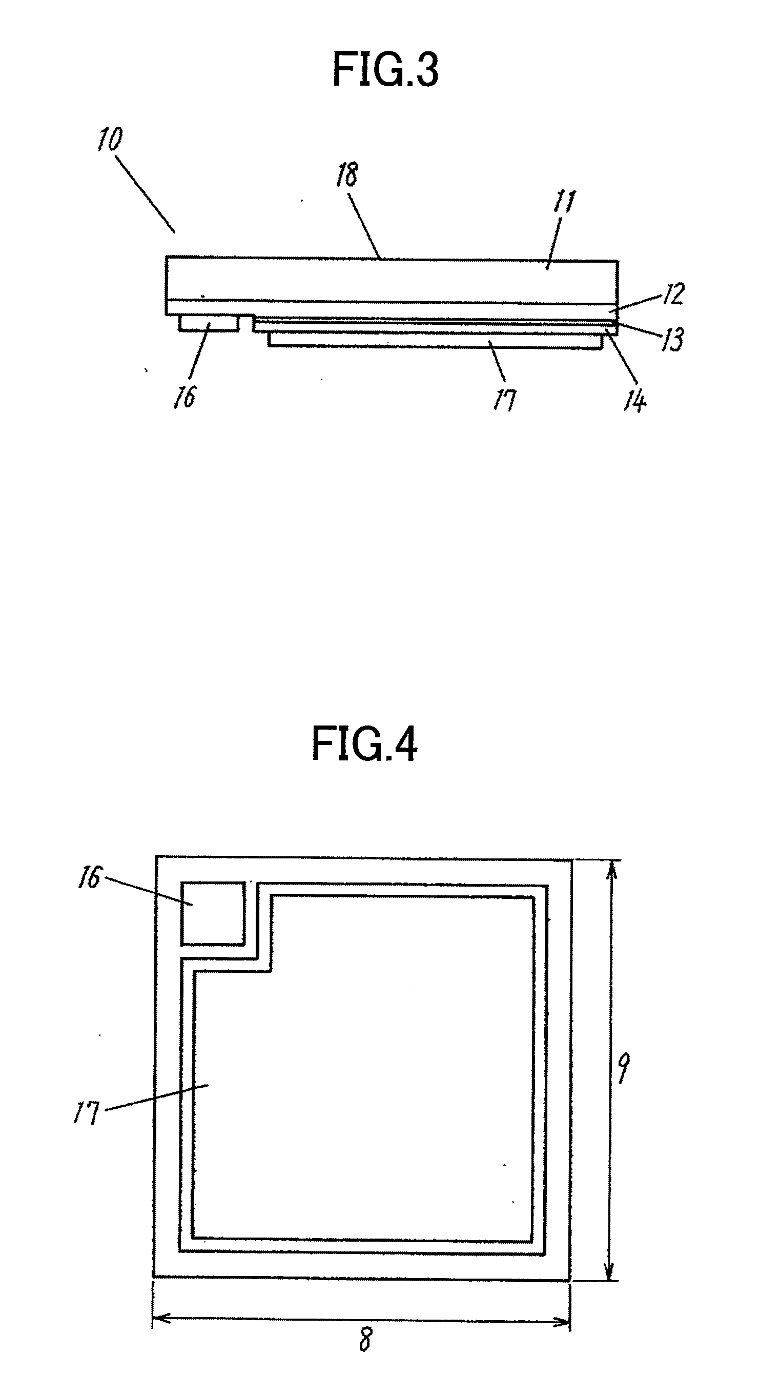
[0055]FIG. 1 shows a semiconductor light-emitting device 1 of the present invention. The semiconductor light-emitting device 1 is structured so that a semiconductor light-emitting element 10 is fixed to a submount 21.

[0056]Although an example using a flip-chip type semiconductor light-emitting element will be described below, the semiconductor light-emitting device of the present invention does not depend on the type of semiconductor light-emitting element. That is, other types of semiconductor light-emitting elements, such as a face-up type, a one-sided electrode type, and a double-sided electrode type, can be used in the present invention.

[0057]Extended electrodes 22, 23 are formed on the submount 21. The extended electrodes are electrodes for supplying a current to the semiconductor light-emitting element 10. The extended electrode 22 is an n-side extended electrode connected to an n-type layer of the semiconductor light-emitting element, and the extended electrode 23 is a p-side...

second embodiment

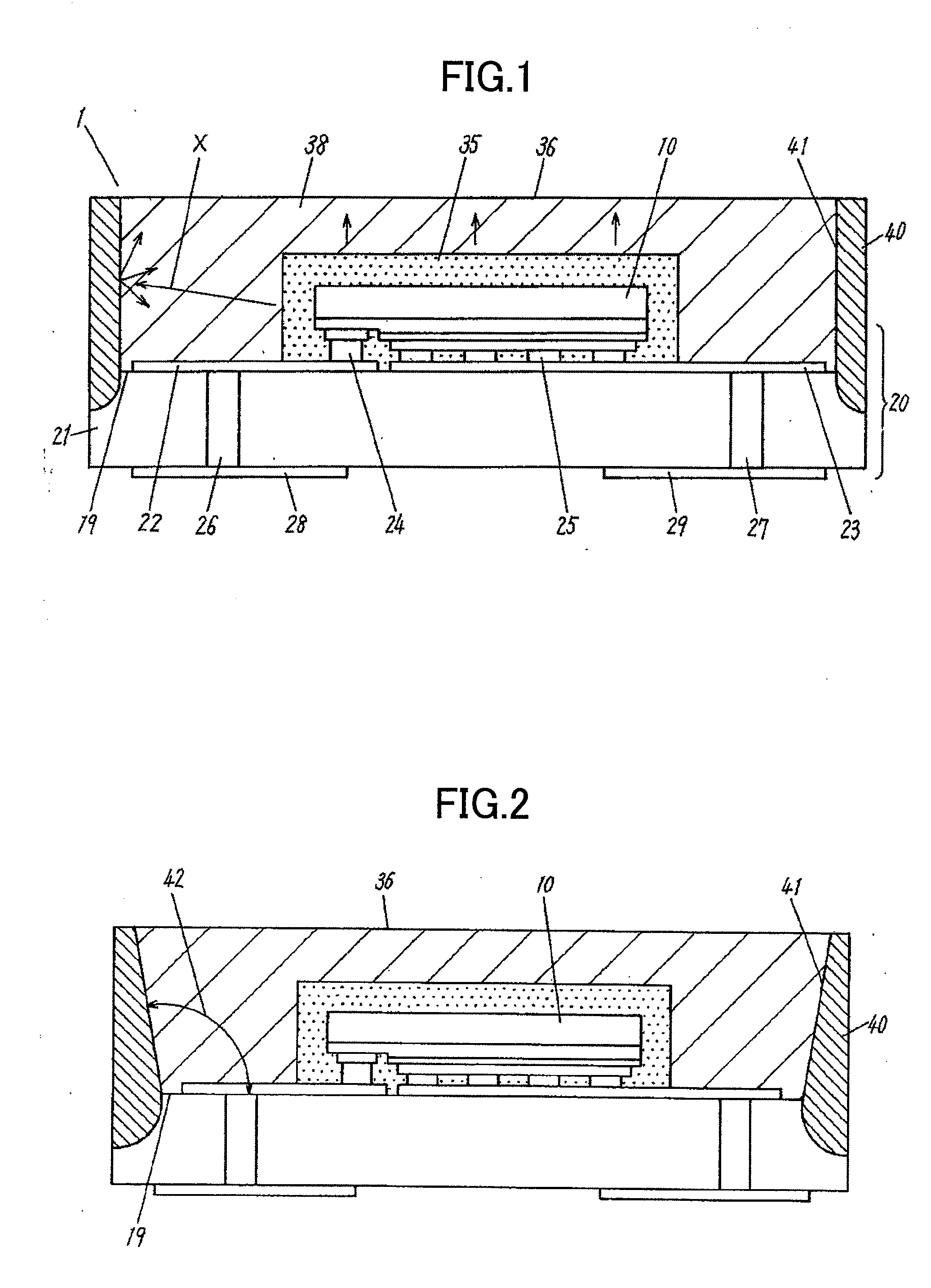
[0105]In the first embodiment, as shown in FIGS. 6A-6B, the sealant 38 is formed over the entire surface of the submount substrate 210 having the semiconductor light-emitting elements placed thereon, and then the groove formation process is performed. This method is capable of processing a large number of substrates in a short time. However, since the sealant is formed over the entire surface of the submount substrate 210, the submount substrate 210 can be subjected to increased stress when the sealant is cured. Excessive stress can bend the submount substrate, or can fracture or crack the portion where the sealant is formed. Thus, the sealant may be formed over each semiconductor light-emitting element.

[0106]FIGS. 9A-9B illustrate a part of a manufacturing method of a semiconductor light-emitting device of the present invention. FIG. 9A is a diagram corresponding to FIG. 6A, and FIG. 9B is the same as FIG. 6B. The manufacturing method of the present embodiment can be exactly the sa...

third embodiment

[0109]A manufacturing method capable of reducing the number of steps will be described in the present embodiment.

[0110]Referring to FIGS. 10A-10C, extended electrodes 22, 23 are formed on a submount substrate 210, bumps 24, 25 are also formed, and semiconductor light-emitting elements 10 are placed thereon (FIG. 10A). A phosphor layer 35 is also formed around each semiconductor light-emitting element 10 (FIG. 10B). These steps are the same as those of the first embodiment.

[0111]Then, a sealant 38 is formed over each semiconductor light-emitting element (FIG. 10C). Although a method of forming the sealant 38 is not limited, the use of a printing method or the like is convenient and quick.

[0112]FIGS. 11A-11C show the subsequent steps. After the sealant is formed, a reflective material 43 is applied and formed over the entire surface of the submount substrate 210 (FIG. 11A). No groove formation process is performed in the present embodiment.

[0113]Surfaces, which serve as light-emitting...


PUM


Abstract

Light from a semiconductor light-emitting element travels in all directions. Thus, light that travels in the directions other than a lighting direction cannot be used effectively. Means for forming a semiconductor light-emitting element having tilted side surfaces, and forming a reflective layer on the tilted side surfaces has been proposed. However, since the tilted surfaces are formed by an etching method or the like, it takes a long time to form the tilted surfaces, and it is difficult to control the tilted surfaces. As a solution to these problems, semiconductor light-emitting elements are placed on a submount substrate and sealed with a sealant, and then a groove is formed in a portion between adjoining ones of the semiconductor light-emitting elements. The grooves formed are filled with a reflective material, and a light-emitting surface is polished. Then, the submount substrate is divided into individual semiconductor light-emitting devices. Thus, a semiconductor light-emitting device having a reflective layer on its side surfaces can be obtained.

Description

TECHNICAL FIELD[0001]The present invention relates to semiconductor light-emitting elements in which a reflective layer is provided on the side surfaces of a sealant in order to effectively use light that is emitted from the side surfaces of the semiconductor light-emitting element, and semiconductor light-emitting devices using the same.BACKGROUND ART[0002]Semiconductor light-emitting elements emit light from a light-emitting layer that is formed by p-type and n-type semiconductors having an active layer therebetween. Thus, light is emitted in all directions. However, in many applications using the semiconductor light-emitting elements as light sources, it is often desired that light be emitted in one direction. In such cases, light that travels in directions different from the radiation direction is wasted. In order to efficiently use light, it is preferable to reflect such light toward a light-emitting surface of the semiconductor light-emitting element.[0003]As a solution to thi...

Claims


Application Information

Patent Timeline
Patent Type & Authority Applications(United States)
IPC IPC(8): H01L33/52H01L33/60H01L21/78H01L33/54
CPCH01L33/54H01L33/60H01L24/97H01L2224/13H01L2224/48091H01L2224/45144H01L2924/00014H01L2924/00H01L2224/04042H01L2224/05111H01L2224/05155H01L2224/05169H01L2224/05573H01L2224/0558H01L2224/05624H01L2224/05639H01L2224/05666H01L2224/14H01L2224/16225H01L2224/32245H01L2224/48247H01L2224/73265H01L2224/97H01L2924/12035H01L2924/12042H01L2924/181H01L2924/00012
Inventor IDE, YOSHIYUKIKAMEI, HIDENORIYONEKURA, ISAMUOBARA, KUNIHIKONAKAHARA, KOICHINAKATSU, KOUJITOOYA, YOSHIROUKITAZONO, TOSHIROUMAEDA, TOSHIHIDEKOYA, KENICHISHIRAHATA, TAKAHIRO
Owner PANASONIC CORP
Why Eureka
Try Eureka