Planar plasmonic device for light reflection, diffusion and guiding

Inactive Publication Date: 2010-10-14
LIGHTWAVE POWER
View PDF5 Cites 50 Cited by
  • Summary
  • Abstract
  • Description
  • Claims
  • Application Information

AI Technical Summary

Problems solved by technology

In terms of economic efficiency, the cost of an absorbing layer is related to both the raw material cost and the manufacturing cost.
While absorption efficiency increases with thickness, the cost of solar cell production increases with increased thickness.
Further complicating the trade-offs between energy conversion efficiency a

Method used


Image

  • Planar plasmonic device for light reflection, diffusion and guiding
  • Planar plasmonic device for light reflection, diffusion and guiding
  • Planar plasmonic device for light reflection, diffusion and guiding

Examples


Embodiment Construction

Definitions

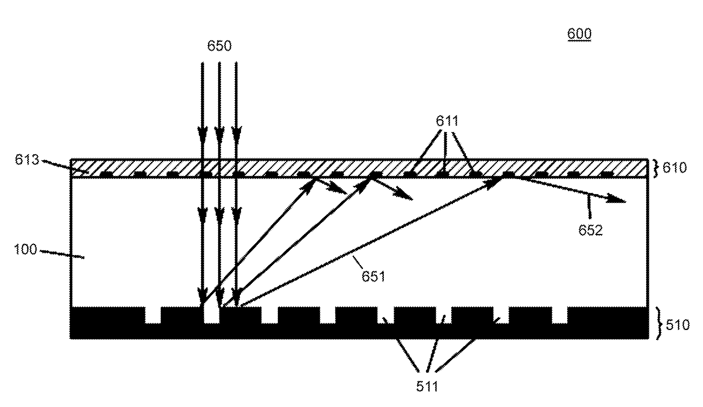
[0042]Integrated solar cell: We refer herein to a complete solar cell assembly of layers as an “integrated solar cell”. The term integrated solar cell, includes integrated structures made using both conventional semiconductor manufacturing methods, e.g. photolithography and vapor deposition, as well as layers manufactured in part or entirely by more recent fabrication methods, such as for example, nanofabrication methods.

[0043]Solar cell layer: The absorber of an integrated solar cell is referred to interchangeably herein as a “solar cell layer”. It is understood that one or more solar cell layers are electrically coupled within an integrated solar cell to provide an integrated solar cell electrical output voltage across an integrated solar cell positive terminal and an integrated solar cell negative terminal. In some embodiments a metal film present for optical reasons can also, but not necessarily, provide as an electrical connection to a solar cell layer.

[0044]Modifica...


PUM


Abstract

A planar plasmonic device includes a first material layer having a surface configured to receive at least one photon of incident light. A patterned plasmonic nanostructured layer is disposed adjacent and optically coupled to the first material layer. The patterned plasmonic nanostructured layer includes a selected one of: a) at least a portion of a surface of the patterned plasmonic nanostructured layer includes a textured surface, and b) at least one compound nanofeature including a first material disposed adjacent to a second material within the compound nanofeature.

Description

CROSS-REFERENCE TO RELATED APPLICATIONS[0001]This application claims priority to and the benefit of co-pending U.S. provisional patent application Ser. No. 61 / 168,292, PLANAR PLASMONIC DEVICE FOR LIGHT REFLECTION, DIFFUSION AND GUIDING, filed Apr. 10, 2009, and co-pending U.S. provisional patent application Ser. No. 61 / 177,449, PATTERNED PLANAR DEVICES AS INTERMEDIATE LIGHT DISTRIBUTING AND GUIDING LAYERS IN SOLAR CELLS, filed May 12, 2009, which applications are incorporated herein by reference in their entirety.FIELD OF THE INVENTION[0002]The invention relates to a planar plasmonic device in general and particularly to a planar plasmonic device employing a textured surface or a compound nanofeature.BACKGROUND OF THE INVENTION[0003]The energy conversion efficiency and cost of a photovoltaic cell is directly related to the thickness of the absorbing layer. The importance of the thickness to conversion efficiency arises from the physics of the absorption process as described by Beer'...

Claims


Application Information

Patent Timeline
IPC IPC(8): G02B5/02
CPCB82Y20/00G02B5/008H01L31/056H01L31/0527Y02E10/52H01L31/02168
Inventor JI, JINSPITZER, MARK B.KAUFMAN, LAWRENCE A.
Owner LIGHTWAVE POWER
Why Eureka
Try Eureka