
Eureka
For R&D, Eureka makes reading and utilizing patents & technical documents easy.
Eureka AIR
Designed for self-driven R&D workflows. Generate viable solutions, solve complex R&D challenges, empower your innovation with AI.

Eureka Materials
Designed for material experts only. Revolutionize your material R&D, from search, analyze, to developing new materials.

TechResearch
Generate reliable direction feasibility study reports for your R&D in just a few steps.

TechSeek
Discover and master advanced knowledge NOW. Basics, ideas, possibilities, all at once.

TechMind
As an expert in R&D Theories, TechMind can generates customized viable solutions instantly.

TechRisk
Analyze your overall solution with one click, know your potential R&D risks in advance.

TechMonitor
Get weekly tech updates, stay abreast of the latest tech innovations and key insights.
Techniques for providing a semiconductor memory device
- Summary
- Abstract
- Description
- Claims
- Application Information
AI Technical Summary
Problems solved by technology
Method used
Image

Examples
Embodiment Construction
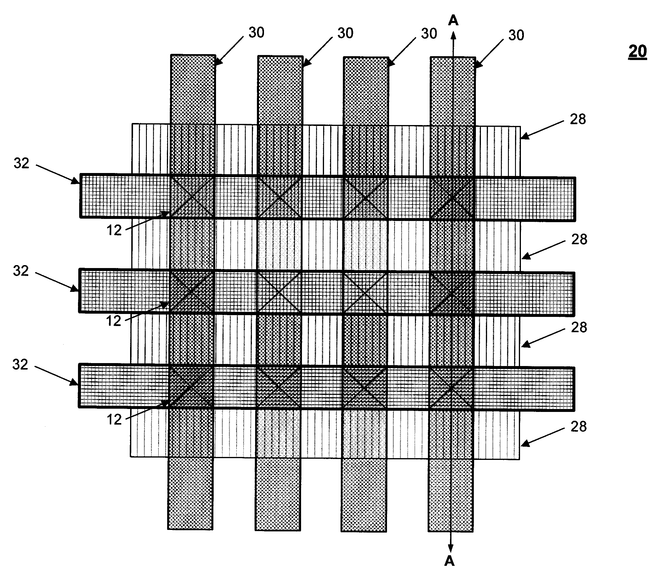
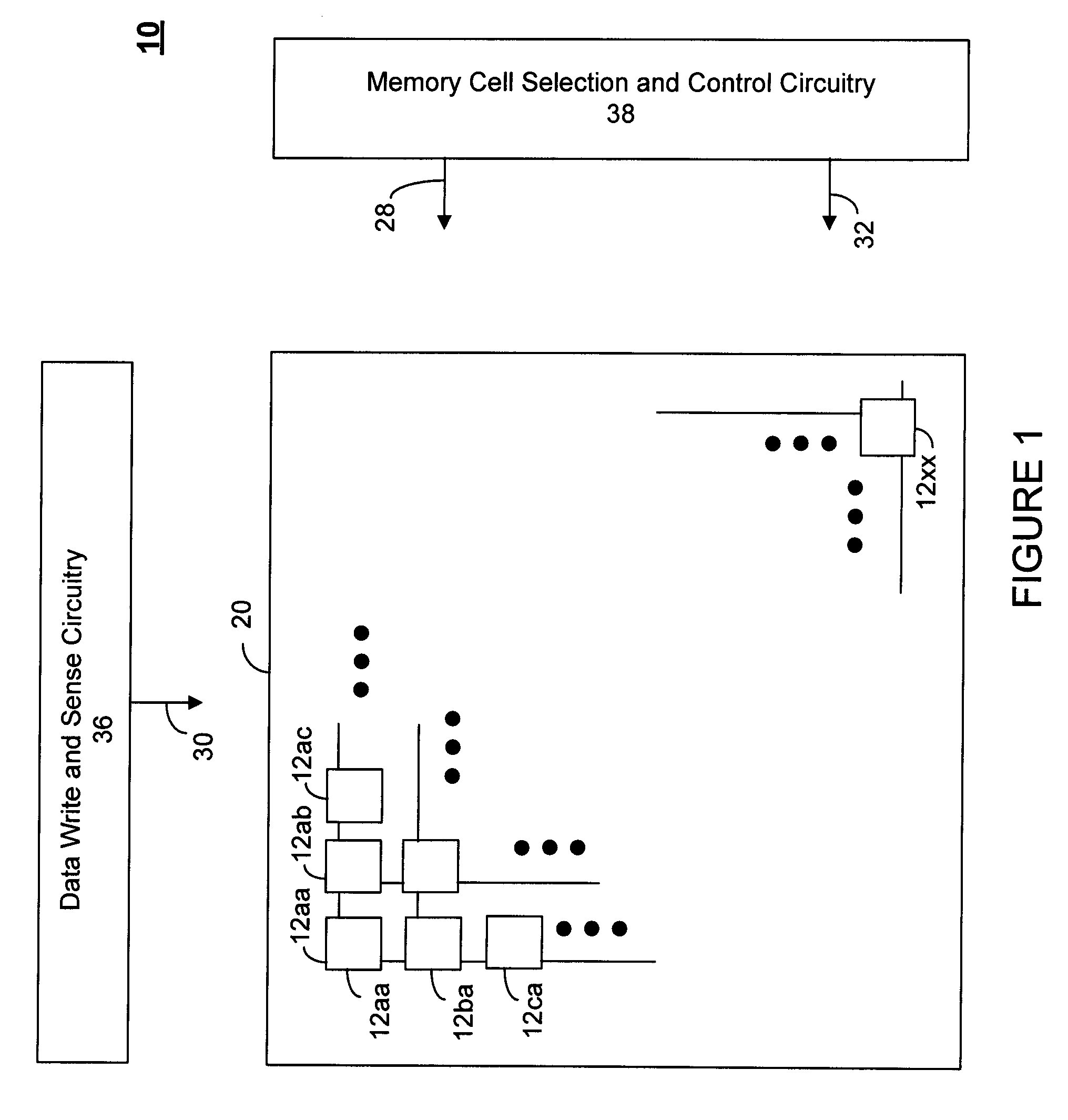
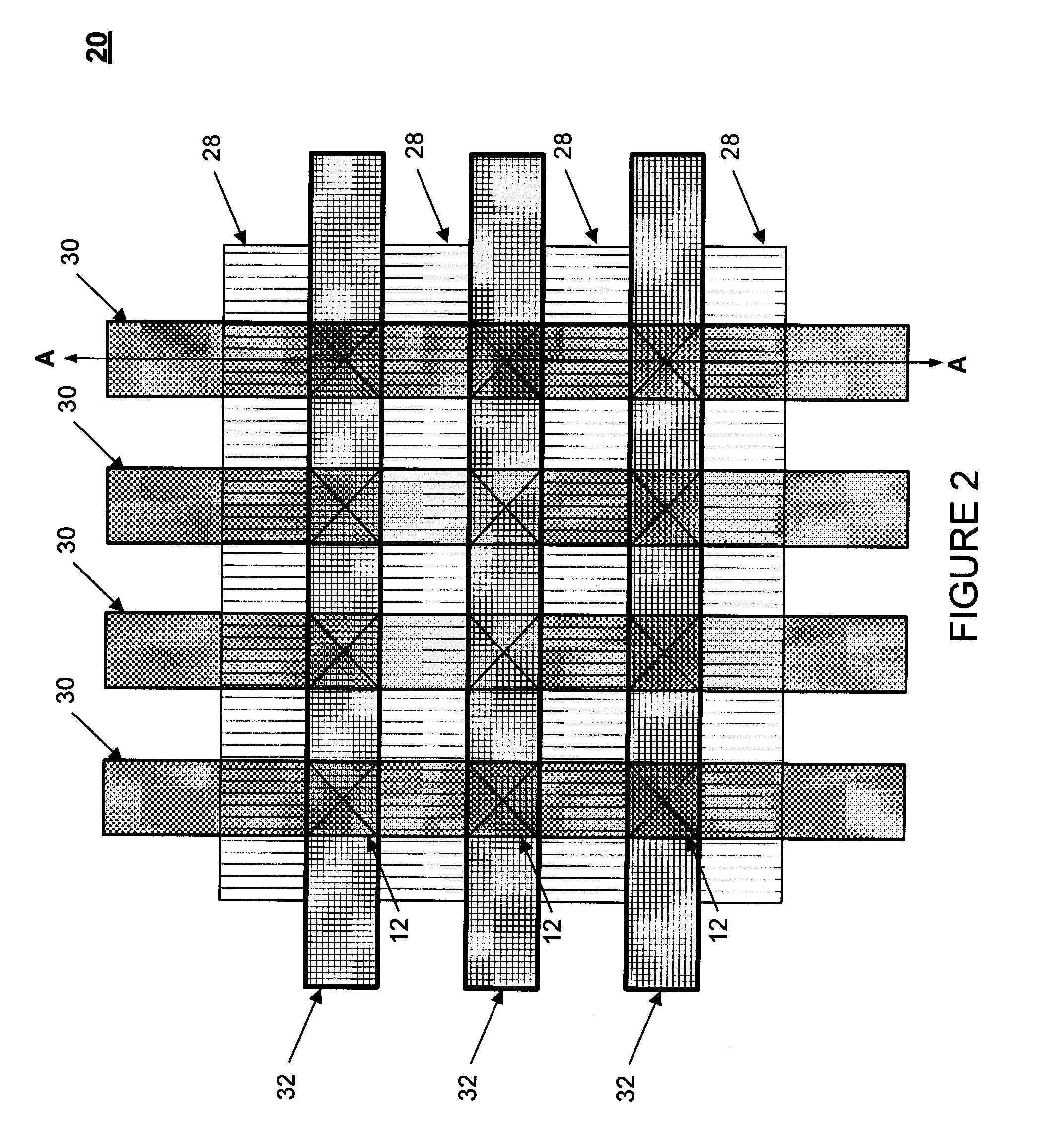
[0042]Referring to FIG. 1, there is shown a schematic block diagram of a semiconductor memory device 10 comprising a memory cell array 20, data write and sense circuitry 36, and memory cell selection and control circuitry 38 in accordance with an embodiment of the present disclosure. The memory cell array 20 may comprise a plurality of memory cells 12 each connected to the memory cell selection and control circuitry 38 via a word line (WL) 28 and / or a source line (EN) 32, and the data write and sense circuitry 36 via a bit line (CN) 30. It may be appreciated that the bit line (CN) 30 and the source line (EN) 32 are designations used to distinguish between two signal lines and they may be used interchangeably. The data write and sense circuitry 36 may read data from and may write data to selected memory cells 12. In an exemplary embodiment, the data write and sense circuitry 36 may include a plurality of data sense amplifiers. Each data sense amplifier may receive at least one bit li...
PUM
 Abstract
Description
Claims
Application Information
 - R&D Engineer
- R&D Manager
- IP Professional
- Industry Leading Data Capabilities
- Powerful AI technology
- Patent DNA Extraction
Browse by: Latest US Patents, China's latest patents, Technical Efficacy Thesaurus, Application Domain, Technology Topic, Popular Technical Reports.
© 2024 PatSnap. All rights reserved.Legal|Privacy policy|Modern Slavery Act Transparency Statement|Sitemap|About US| Contact US: help@patsnap.com