Multi-layer film and electronic device shell having same
- Summary
- Abstract
- Description
- Claims
- Application Information
AI Technical Summary
Problems solved by technology
Method used
Image

Examples
first embodiment
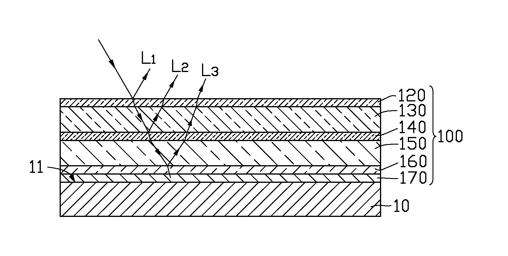
[0012]Referring to FIG. 1, an exemplary multi-layer film 100 in accordance with a first embodiment is shown. The multi-layer film 100 includes in sequence a first metallic layer 120, a first medium layer 130, a second metallic layer 140, a second medium layer 150, a third metallic layer 160, and a light absorbing layer 170. The first metallic layer 120, first medium layer 130, second metallic layer 140, second medium layer 150, third metallic layer 160 and the light absorbing layer 170 have top surfaces and bottom surfaces parallel to each other. The light absorbing layer 170 is configured to cling (adhere) to a surface 11 of a substrate 10. In this description, the combination of the multi-layer film 100 and the substrate 10 is referred to as a “multi-layer film structure.”
[0013]The first metallic layer 120, the second metallic layer 140, and the third metallic layer 160 each contain a material selected from a group consisting of aluminum, nickel, chromium, and alloy of nickel and ...
second embodiment
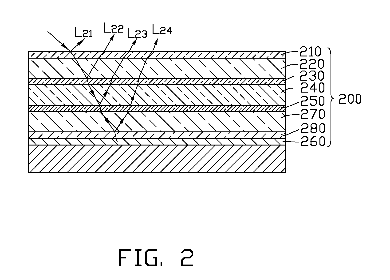
[0017]Referring to FIG. 2, an exemplary multi-layer film 200 in accordance with a second embodiment is shown. The multi-layer film 200 is similar in principle to the multi-layer film 100 described above. However, the multi-layer film 200 includes in sequence a first metallic layer 210, a first medium layer 220, a second metallic layer 230, a second medium layer 240, a third metallic layer 250, a third medium layer 270, a fourth metallic layer 280, and a light absorbing layer 260. The first metallic layer 210, the second metallic layer 230, the third metallic layer 250 and the fourth metallic layer 280 are capable of reflecting incident light and allowing another part of the incident light to transmit therethrough to produce a first reflected light L21, a second reflected light L22, a third reflected light L23, and a fourth reflected light L24, respectively. Interferences occur between the first reflected light L21, the second reflected light L22, the third reflected light L23 and th...
PUM
| Property | Measurement | Unit |
|---|---|---|
| Thickness | aaaaa | aaaaa |
| Thickness | aaaaa | aaaaa |
| Thickness | aaaaa | aaaaa |
Abstract
Description
Claims
Application Information
 - R&D Engineer
- R&D Manager
- IP Professional
- Industry Leading Data Capabilities
- Powerful AI technology
- Patent DNA Extraction
Browse by: Latest US Patents, China's latest patents, Technical Efficacy Thesaurus, Application Domain, Technology Topic.
© 2024 PatSnap. All rights reserved.Legal|Privacy policy|Modern Slavery Act Transparency Statement|Sitemap