Accurate Approximation of Resistance in a Wire with Irregular Biasing and Determination of Interconnect Capacitances in VLSI Layouts in the Presence of Catastrophic Optical Proximity Correction

a technology of irregular biasing and accurate approximation of resistance, applied in the field of computer modeling of chip designs, can solve the problems of large amount of memory and processor resources, large amount of electrical parasitic values, and inability to accurately reflect the width of the actual wire, so as to reduce memory and performance consumption

Active Publication Date: 2010-10-14
SIEMENS PROD LIFECYCLE MANAGEMENT SOFTWARE INC
View PDF9 Cites 3 Cited by
  • Summary
  • Abstract
  • Description
  • Claims
  • Application Information

AI Technical Summary

Benefits of technology

[0008]Therefore, a need exists for a way to reduce memory and performance consumption when calculating parametric electrical values due to width bias for design validation.

Problems solved by technology

However, due to modern chip fabrication processes, these widths do not always reflect the width of the actual wire after fabrication.
In particular, those DA applications that extract electrical parasitic values often require large amounts of memory and processor resources because many of the calculations performed require design context data to account for contextually sensitive width biasing.
However, this method requires double the memory.
Determining the spacing to one side and saving the spacing dependent bias for that side until the spacing to the other side is determined, creates a problem.
The problem is that it may be too late for the DA application to calculate capacitance to the first neighboring shape because the first neighboring shape has been lost due to the examination process.
Because of this effect, DA applications must consume considerable storage remembering the important information and sustain a performance loss organizing that information.

Method used


Image

  • Accurate Approximation of Resistance in a Wire with Irregular Biasing and Determination of Interconnect Capacitances in VLSI Layouts in the Presence of Catastrophic Optical Proximity Correction
  • Accurate Approximation of Resistance in a Wire with Irregular Biasing and Determination of Interconnect Capacitances in VLSI Layouts in the Presence of Catastrophic Optical Proximity Correction
  • Accurate Approximation of Resistance in a Wire with Irregular Biasing and Determination of Interconnect Capacitances in VLSI Layouts in the Presence of Catastrophic Optical Proximity Correction

Examples


Embodiment Construction

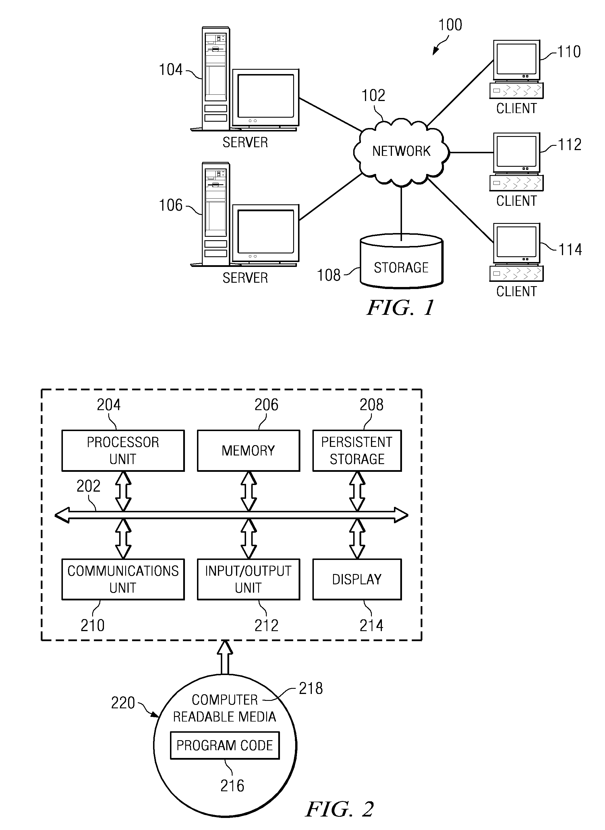
[0027]With reference now to the figures, and in particular with reference to FIGS. 1-2, exemplary diagrams of data processing environments are provided in which illustrative embodiments may be implemented. It should be appreciated that FIGS. 1-2 are only exemplary and are not intended to assert or imply any limitation with regard to the environments in which different embodiments may be implemented. Many modifications to the depicted environments may be made.

[0028]FIG. 1 is a pictorial representation of a network of data processing systems in which illustrative embodiments may be implemented. Network data processing system 100 is a network of computers in which the illustrative embodiments may be implemented. Network data processing system 100 contains network 102, which is the medium used to provide communication links between various devices and computers connected together within network data processing system 100. Network 102 may include connections, such as wire, wireless commu...


PUM


Abstract

The Width Bias Calculator (WBC) calculates electrical values by effectively averaging the electrical values to either side of a target wire shape whereby values are approximated for design validation without a significant impact on performance or memory consumption.

Description

BACKGROUND[0001]1. Field[0002]The disclosure relates generally to computer modeling of chip designs and more specifically to determination of resistance and parasitic capacitance by Design Automation Software Applications.[0003]2. Description of the Related Art[0004]Wire shapes in a wiring layout are defined with a certain width by the designer. However, due to modern chip fabrication processes, these widths do not always reflect the width of the actual wire after fabrication. This variance between design and fabrication width is referred to as width bias. The width bias, of a wire fabricated on a chip with the latest small wire geometry, has become dependent on the spacing to neighboring wires. In order to validate a design to the design specification, electrical values, such as parasitic capacitance and resistance values, must be calculated each time a change is made to a wiring layout.[0005]In order to accurately calculate parasitic capacitance and resistance values, Design Autom...

Claims


Application Information

Patent Timeline
Patent Type & Authority Applications(United States)
IPC IPC(8): G06F17/50
CPCG06F17/5081G06F30/398
Inventor DEWEY, III, LEWIS WILLIAMELFADEL, IBRAHIM M.WIDIGER, DAVID J.
Owner SIEMENS PROD LIFECYCLE MANAGEMENT SOFTWARE INC
Why Eureka
Try Eureka